The Quest for More Processing Power, Part One: "Is the single core CPU doomed?"
by Johan De Gelas on February 8, 2005 4:00 PM EST- Posted in
- CPUs
When a CPU becomes a sieve
The real problem is leakage power, and the Intel power graph below illustrates this perfectly.
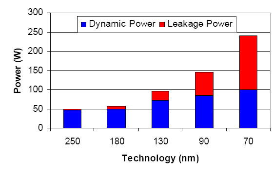
Fig 2. "Leakage power grows exponentially ".
As you can see, dynamic power - which does useful work - has increased relatively slowly despite the increase in CPU complexity. Leakage power, however, increases exponentially, and not linearly. It has grown quickly from a "minor nuisance" to a "circuit killing monster".
Leakage is comparable to a small hole in a waterhose of a firefighter. The more pressure (i.e. the higher the core voltage), the bigger the hole gets, and thus, the more water that leaks to the ground. The thinner the walls of the tube (i.e. smaller process technology), the quicker the holes become bigger, and the more water you lose, the harder the pumps must work to get the same amount of water to extinguish the fire. If the pumps overheat, you better throttle them down, or they will cease to work after a while.
Power Leakage happens as a part of the current, which is supposed to make our transistors switch leaks away in the substrate and finally in the ground. There are several leakage currents, but the two most important ones are the gate oxide tunnelling current and sub-threshold leakage.[3]
![]()
Fig 3. I3 is the Gate oxide tunnelling currents, I2 is the Sub-threshold leakage current
Gate oxide tunnelling (I3) currents get more important with smaller process technology as the gate oxide that is supposed to insulate the transistor becomes thinner and thinner. As a result, current that is going through the transistors leaks away - the gate oxide becomes a sieve instead of being the "wall of a tube".
Sub-threshold leakage (I2) transistor is the leakage current flowing through the transistor when it is supposed to be turned off. To understand this, we got to back to basic transistor technology.
Normally, a voltage threshold of x volts is needed to get current across the transistor, with x volts being the threshold. This way, the transistor is being used as a switch with a binary function: more or equal to threshold voltage = ON = 1, less than the threshold voltage = OFF.
The point that you have to remember is this: ideally, as long as the threshold voltage is not reached, no current should run through the transistor. However, as transistors and interconnects get smaller and smaller (smaller process technology), the insulation between drain and source gets worse and worse. As a result, a small leakage current gets through the transistor (I 2) even though the threshold voltage is not reached (the Transistor is off).
That subthreshold leakage has become a major problem, which has been made clear by Shekhar Borkar [5] (Intel Fellow, Director of Circuit Research). He illustrated this by the logarithmic graph below.
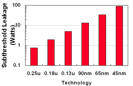
Fig 4. Subthreshold leakage - notice the logarithmic scale!
Subthreshold leakage was only a small problem at the time of Willamette - the leakage problem wasted a few watts at 180 nm. The graph is based on Moore's law: every two years, the number of transistors doubles. As you can see, without countermeasures, it wouldn't be interesting to use devices that make use of 45 nm technology. They would simply leak too much power, up to 100 Watts!
And subthreshold leakage is only part of the leakage problem. Together with gate oxide tunnelling, CPUs made of 65 nm technology would leak more power than what they need for making the transistors switch. It is comparable to a fuel tank that has so many holes, causing it to leak more gasoline to the ground than what the fuel pump can pump to the engine.
Let us check the third and last problem for high performance CPUs.
Wire delay
It is hard to imagine that the little wires - the metal interconnects - between transistors can be a limiting factor. About twenty years ago, transistor switching speeds were pretty low, and wire delays were completely ignored. However, as process technology became better, transistors were capable of switching much faster. Right now, the fastest transistors in the labs can attain 100 GHz (the record being around 300-500 GHz) and more. So, transistor switching speed still has a lot of headroom.
The tiny wires between the different transistors are still not the problem. Functional blocks are also wired to the TLBs (Translation Lookaside Buffer) and caches. The real problem is these global wires - they are a lot longer . If the RC delay is too high, the clock speed will have to be reduced to get a working CPU.
The speeds at which signals travel through the global wires (from logic blocks to the caches, for example) are quite a bit slower than what the maximum speed (speed of light) allows. The reason is the resistance (R, Ohm) and capacitive resistance (C) of the wire. As the whole CPU was made with smaller process technology, the wires also shrunk. You probably know from your lessons of physics that resistance increases as the cross section of the wire gets smaller and the length of the wire gets longer. So, if you shrink a wire, the effect of the shorter length is completely negated by the smaller thickness of the wire. You could make the wires thicker, but it wouldn't be easy and that would increase the capacitance of the wire. The result is that wire delay remains, more or less, the same (in nanoseconds).
However, gate switching speed improves a lot with smaller transistors (for example, 100%). So, while RC delay improves with a very small percentage (or nothing all), gates might switch up to 100% (simplified example) faster as process technology improves. The RC delay of the global wires becomes more a bottleneck that makes bumping up the clock speed hard. Modern Integrated Circuits (ICs), such as CPUs, must be partitioned, as a signal can travel for a time slightly less than the length of one clockpulse.


65 Comments
View All Comments
Momental - Wednesday, February 9, 2005 - link
#41, I understood what he meant when he stated that AMD could only be so lucky to have something which was a technological failure, ie: Prescott, sell as well as it has. Even the article clearly summarizes that Prescott in and of itself isn't a piece of junk per se, only that is has no more room for evolution as Intel originally had hoped.#36 wasn't saying that it was a flop sales-wise, quite the contrary. The thing has sold like hotcakes!
I, like many others here, literally got dizzy as I struggled to keep up with all of the technical terminology and mathmetical formulas. My brain is, as of this moment, threatening to strike if I don't get it a better health and retirement plan along with a shorter work week. ;)
Ivo - Wednesday, February 9, 2005 - link
1. About the multiprocessing: Of coarse, there are many (important!) applications, which are more than satisfied with the existing mono-CPU performance. Some other will benefit from dual CPUs. Matrix 2CPU+2GPU combinations could be essential e.g. for stereo-visualization. Probably, desktop machines with enhanced voice/image analytical capabilities could require even more sophisticated CPU Matrices. I suppose, the mono- and multi-CPU solutions will coexist in the near future.2. About the leakage problem: New materials like SOI are part of the solution. Another part are the new techniques. Let us take a lesson from the nature: our blood-transportation system consists of tiny capillaries and much thicker arteries. Maybe it could make sense to combine 65 nm transistors e.g. in the cash memory and 90 nm transistors in the ALU?
Noli - Wednesday, February 9, 2005 - link
"Netburst architecture is very innovative and even genial"genius-like?
If by genial you mean 'having a pleasant or friendly disposition', it sounds weird. It can mean 'conducive to growth' in this context but that's not so intuitive because a) it wasn't and b) at best it was only theoretically genial.
Presumably it's not genial as in 'of or relating to the chin' :)
Agree monolithic was confusing but it was the intel dude who said it - I thought it meant 'large single unit' rather than 'old (as in technology)' as in: increasing processing power by increasing the size and complexity of a single core is now not as efficient as strapping two cores together - a duallithic unit :)
Sorry to be a pedantic twat.
Xentropy - Wednesday, February 9, 2005 - link
Some of the verbage in that final chapter makes me wonder how much better Prescott might have done if Intel had just left out everything 64-bit and developed an entirely different processor for 64-bit. Especially since we won't have a mainstream OS that'll even utilize those instructions for another few months, and it's already been about a year since release, they could have easily gotten away with putting 64-bit off for the next project. It's pretty obvious by now even the 32-bit Prescotts have those 64-bit transistors sitting around. Even if not active, they aren't exactly contributing to the power efficiency of the processor.I think one big reason Intel thinks dual core will be the savior of even the Prescott line is supposedly dual cores running at 3Ghz only require equivalent power draw to a single core at 3.6Ghz and should be just as fast in some situations (multitasking, at least). Dual core at 85% clockspeed will be slower for gaming, though, so dual core Prescott still won't close the gap with AMD for gaming enthusiasts (98% of this site's readership), and may even represent an even further drop in performance per watt. Here's hoping for Pentium-M on the desktop. :>
piroroadkill - Wednesday, February 9, 2005 - link
#36 -- You really didn't read the article and get the point of it. It wasn't a failure from a sales point of view, and this article was not written from a sales point of view, but a technical point of view, and how the Prescott helped in furthering CPU technology.Thus, a failure.
ViRGE - Wednesday, February 9, 2005 - link
Although I think I sank more than I swam, that was a very good and informative article Johan. I just have one request for a future article since I'm guessing the next one is on multi-core tech: will someone at AT run the full AT benchmark suite against a SMP Xeon machine so that we can get a good idea ahead of time what dual-core performance will be like against single core? My understanding is that the Smithfields aren't going to be doing much else new besides putting 2 cores on one die(i.e. no cache sharing or other new tech), so SMP benchmarks should be fairly close to dual-core benchmarks.Griswold - Wednesday, February 9, 2005 - link
Point and case as to why the marketing department is the most important (and powerful) part of any highly successful company. It's not the R&D labs who tell you what works and what comes next, it's the PR team.quidpro - Wednesday, February 9, 2005 - link
Someone needs to make a new Tron movie so I can understand this better.tore - Wednesday, February 9, 2005 - link
Great article, on page 3 you talk about BJT transistor with a base, collector and emitter, since all modern cpu's use mosfets should you talk about a mosfet with a gate, source and drain?Questar - Wednesday, February 9, 2005 - link
"The Pentium 4 "Prescott" is, despite its innovative architecture, a failure."AMD wishes they had a "failure" that sold like Prescott.