NVIDIA Announces the GeForce RTX 30 Series: Ampere For Gaming, Starting With RTX 3080 & RTX 3090
by Ryan Smith on September 1, 2020 1:15 PM EST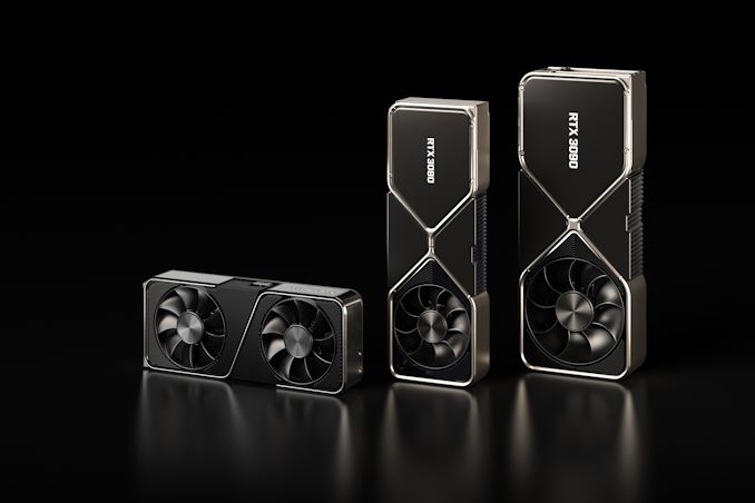
With much anticipation and more than a few leaks, NVIDIA this morning is announcing the next generation of video cards, the GeForce RTX 30 series. Based upon the gaming and graphics variant of NVIDIA’s Ampere architecture and built on an optimized version of Samsung’s 8nm process, NVIDIA is touting the new cards as delivering some of their greatest gains ever in gaming performance. All the while, the latest generation of GeForce will also be coming with some new features to further set the cards apart from and ahead of NVIDIA’s Turing-based RTX 20 series.
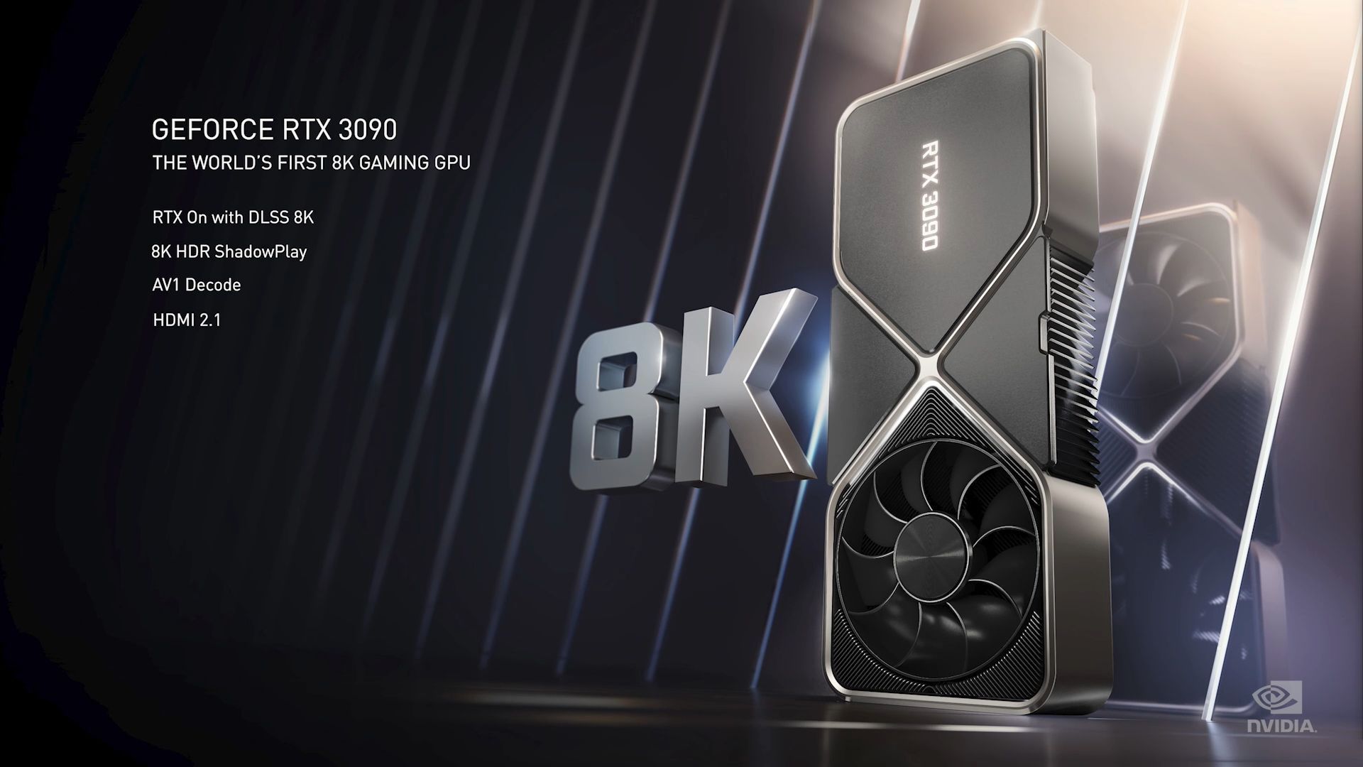
Out of the gate, NVIDIA is announcing the first three cards to make up the new RTX 30 series: the RTX 3090, RTX 3080, and RTX 3070. These cards are all launching within the next month and a half – albeit at slightly separate times – with the RTX 3090 and RTX 3080 leading the charge. The two cards, in turn, will serve as the successors to NVIDIA’s GeForce RTX 2080 Ti and RTX 2080/2080S respectively, hitting new highs in graphics performance, albeit while also hitting new highs in prices in the case of the RTX 3090.
The first card out the door will be the GeForce RTX 3080. With NVIDIA touting upwards of 2x the performance of the RTX 2080, this card will go on sale on September 17th for $700. That will be followed up a week later by the even more powerful GeFoce RTX 3090, which hits the shelves September 24th for $1500. Finally, the RTX 3070, which is being positioned as more of a traditional sweet spot card, will arrive next month at $499.
| NVIDIA GeForce Specification Comparison | ||||||
| RTX 3090 | RTX 3080 | RTX 3070 | RTX 2080 Ti | |||
| CUDA Cores | 10496 | 8704 | 5888 | 4352 | ||
| Boost Clock | 1.7GHz | 1.71GHz | 1.73GHz | 1545MHz | ||
| Memory Clock | 19.5Gbps GDDR6X | 19Gbps GDDR6X | 16Gbps GDDR6 | 14Gbps GDDR6 | ||
| Memory Bus Width | 384-bit | 320-bit | 256-bit | 352-bit | ||
| VRAM | 24GB | 10GB | 8GB | 11GB | ||
| Single Precision Perf. | 35.7 TFLOPs | 29.8 TFLOPs | 20.4 TFLOPs | 13.4 TFLOPs | ||
| Tensor Perf. (FP16) | 143 TFLOPs | 119 TFLOPs | 82 TFLOPs | 114 TFLOPs | ||
| Tensor Perf. (FP16-Sparse) | 285 TFLOPs | 238 TFLOPs | 163 TFLOPs | 114 TFLOPs | ||
| Ray Perf. | 69 TFLOPs | 58 TFLOPs | 40 TFLOPs | ? | ||
| TDP | 350W | 320W | 220W | 250W | ||
| GPU | GA102 | GA102 | GA104? | TU102 | ||
| Transistor Count | 28B | 28B | ? | 18.6B | ||
| Architecture | Ampere | Ampere | Ampere | Turing | ||
| Manufacturing Process | Samsung 8nm | Samsung 8nm | Samsung 8nm | TSMC 12nm "FFN" | ||
| Launch Date | 09/24/2020 | 09/17/2020 | 10/2020 | 09/20/2018 | ||
| Launch Price | MSRP: $1499 | MSRP: $699 | MSRP: $499 | MSRP: $999 Founders $1199 |
||
Ampere for Gaming: GA102
As is traditionally the case for NVIDIA, this morning’s public presentation was not an architectural deep dive. Though the purely virtual presentation was certainly a change of pace for a company who treats every video card launch like a party, NVIDIA stuck to their successful launch playbook. That means a lot of demonstrations, testimonials, and promotional videos, along with some high-level overviews of several of the technologies and engineering design decisions that went into making their latest generation of GPUs. The net result is that we have a decent idea of what’s in store for the RTX 30 series, but we’ll have to wait for NVIDIA to offer some deep dive technical briefings to fill in the blanks and get to the heart of matters in true AnandTech style.
At a high level, Ampere and the GA102 GPU being used in these top-tier cards brings several major hardware advancements to NVIDIA’s lineup. The biggest of which is the ever-shrinking size of transistors, thanks to a customized version of Samsung's 8nm process. We only have limited information about this process – mostly because it hasn't been used too many places – but at a high level it's Samsung's densest traditional, non-EUV process, derived from their earlier 10nm process. All told, NVIDIA has ended up as a bit of a latecomer in moving to smaller processes, but as the company has re-developed an affinity for shipping large GPUs first, they need higher wafer yields (fewer defects) to get chips out the door.
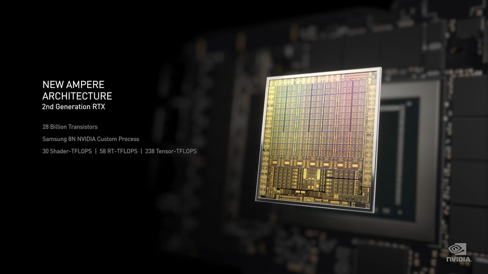
In any case, for NVIDIA’s products Samsung's 8nm process is a full generational jump from their previous process, TSMC’s 12nm “FFN”, which itself was an optimized version of TSMC's 16nm process. So NVIDIA’s transistor densities have gone up significantly, leading to a 28B transistor chip in the case of GA102, which is reflected in the sheer number of CUDA cores and other hardware available. Whereas mid-generation architectures like Turing and Maxwell saw most of their gains at an architectural level, Ampere (like Pascal before it) benefits greatly from a proper jump in lithographic processes. The only hitch in all of this is that Dennard Scaling has died and isn’t coming back, so while NVIDIA can pack more transistors than ever into a chip, power consumption is creeping back up, which is reflected in the cards' TDPs.
NVIDIA hasn’t given us specific die sizes for GA102, but based on some photos we’re reasonably confident it’s over 500mm2. Which is notably smaller than the ridiculously-sized 754mm2 TU102, but it’s still a sizable chip, and among the largest chips produced at Samsung.
Moving on, let’s talk about the Ampere architecture itself. First introduced this spring as part of NVIDIA’s A100 accelerator, until now we’ve only seen Ampere from a matching compute-oriented perspective. GA100 lacked several graphics features so that NVIDIA could maximize the amount of die space allocated to compute, so while graphics-focused Ampere GPUs like GA102 are still a member of the Ampere family, there are a significant number of distinctions or differences between the two. Which is to say that NVIDIA was able to keep a lot under wraps about the gaming side of Ampere until now.
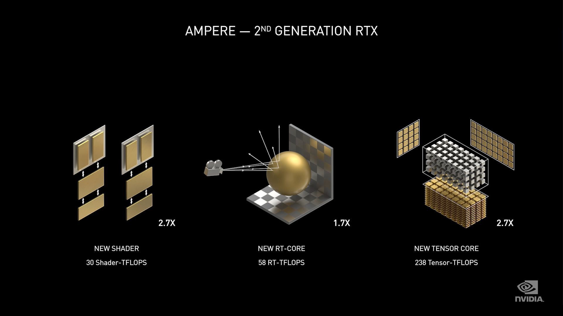
From a compute perspective, Ampere looked a fair bit like Volta before it, and the same can be said from a graphics perspective. GA102 doesn’t introduce any exotic new functional blocks like RT cores or tensor cores, but their capabilities and relative sizes have been tweaked. The most notable change here is that, like Ampere GA100, the gaming Ampere parts inherit updated and more powerful tensor cores, which NVIDIA calls their third generation tensor cores. A single Ampere tensor core can provide double the tensor throughput of a Turing tensor core, with NVIDIA essentially consolidating what was 8 tensor cores per SM into 4. So per SM, the tensor core performance is stable, and while this has some ramifications for how things work under the hood, for gaming Ampere parts you're looking at roughly just as many tensor ALUs per SM. Note that this is different from how Big Ampere (GA100) is configured; that part has 8 of the 3rd gen tensor cores per SM, doubling its performance over its predecessor.
Meanwhile NVIDIA has confirmed the tensor cores going into GA102 and other Ampere graphics GPUs also support sparsity for more performance, and in fact it's these figures that NVIDIA is quoting in today's presentation. So NVIDIA has not held back here in terms of tensor core features. But to a certain degree this does mean that the presentation was misleading – or at least not-apples-to-apples – as Turing didn't support sparsity. If you run "dense" arrays, Ampere is only a mild improvement over Turing.
Overall, this focus on tensor core performance underscores NVIDIA’s commitment to deep learning and AI performance, as the company sees deep learning as not just a driver of their datacenter business, but their gaming business as well. We only have to go as far as NVIDIA’s Deep Learning Super Sampling (DLSS) tech to see why; DLSS relies in part on the tensor cores to deliver as much performance as possible, and NVIDIA is still looking at more ways to put their tensor cores to good use.
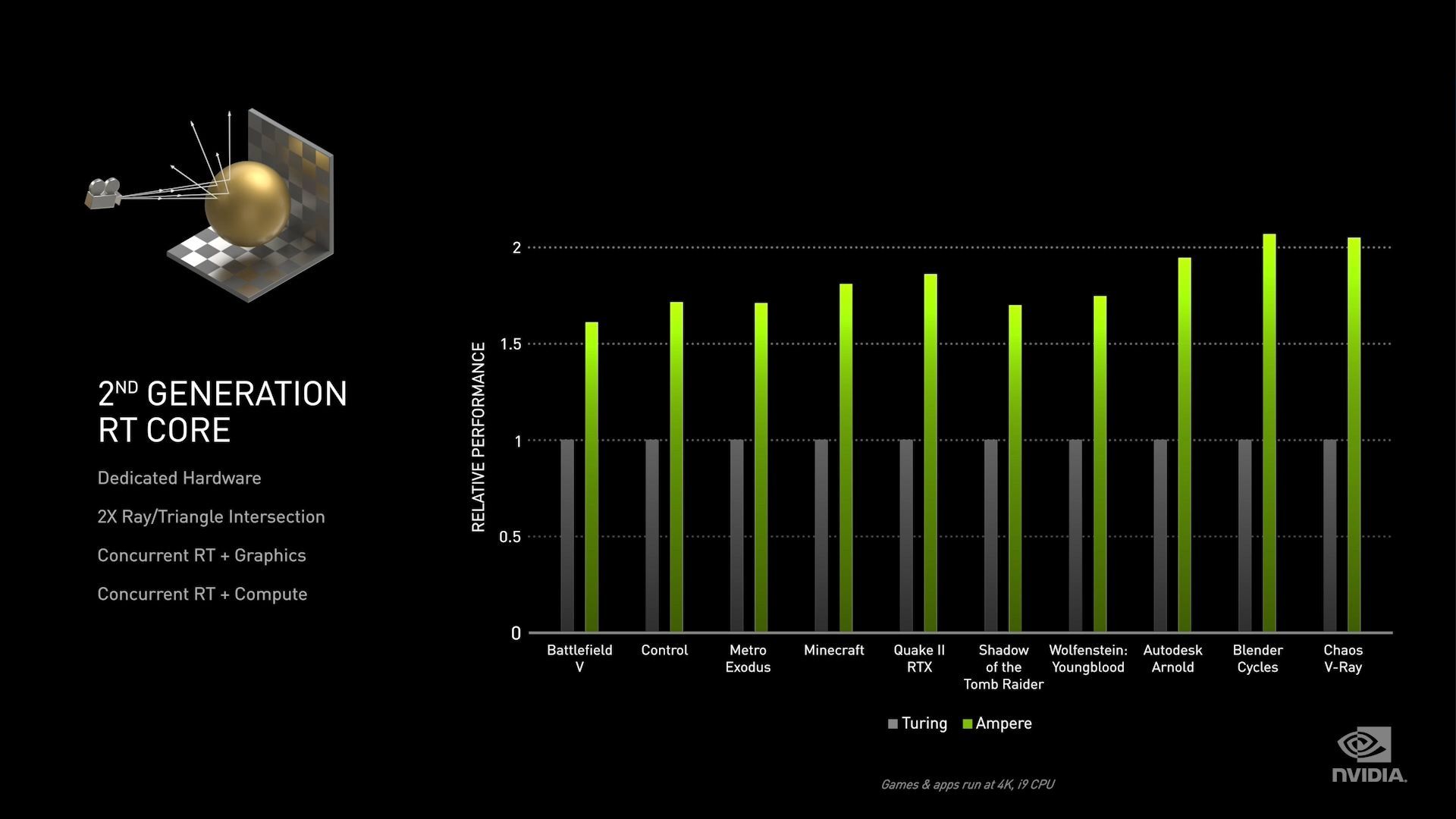
The ray tracing (RT) cores have also been beefed up, though to what degree we’re not certain. Besides having more of them overall by virtue of GA102 having a larger number of SMs, the individual RT cores are said to be up to 2x faster, with NVIDIA presumably specifically quoting ray/triangle intersection performance. There are also some brief notes about RT core concurrency in NVIDIA's presentation slides, but the company didn't go into any real detail on the subject in the brief presentation, so we're waiting on technical briefings for more details.
Overall, faster RT cores is very good news for the gaming industry’s ray tracing ambitions, as ray tracing had a heavy performance cost on RTX 20 series cards. Now with that said, nothing NVIDIA does is going to completely eliminate that penalty – ray tracing is a lot of work, period – but more and rebalanced hardware can help bring that cost down.
Last but certainly not least, we have the matter of the shader cores. This is the area that's the most immediately important to gaming performance, and also the area where NVIDIA has said the least today. We know that the new RTX 30 series cards pack an incredible number of FP32 CUDA cores, and that it comes thanks to what NVIDIA is labeling as "2x FP32" in their SM configuration. As a result, even the second-tier RTX 3080 offers 29.8 TFLOPs of FP32 shader performance, more than double the last-gen RTX 2080 Ti. To put it succinctly, there is an incredible number of ALUs within these GPUs, and frankly a lot more than I would have expected given the transistor count.
Shading performance is not everything, of course, which is why NVIDIA's own performance claims for these cards isn't nearly as high as the gains in shading performance alone. But certainly shaders are a bottleneck much of the time, given the embarrassingly parallel nature of computer graphics. Which is why throwing more hardware (in this case, more CUDA cores) at the problem is such an effective strategy.
The big question at this point is how these additional CUDA cores are organized, and what it means for the execution model within an SM. We're admittedly getting into more minute technical details here, but how easily Ampere can fill those additional cores is going to be a critical factor in how well it can extra all those teraFLOPs of performance. Is this driven by additional IPC extraction within a warp of threads? Running further warps? Etc.
On a final note, while we're waiting for more technical information on the new cards, it's noteworthy that none of NVIDIA's spec sheets or other materials mention any additional graphics features in the cards. To NVIDIA's credit, Turing was already well ahead of the curve, offering the features that would become the new DirectX 12 Ultimate/feature level 12_2 set over two years before any other vendor. So with Microsoft and the rest of the field just now catching up, there's no immediate higher feature set for NVIDIA to aspire to. Still, it's unusual to not see NVIDIA pull a new graphics feature or two out of its proverbial hat just to wow the crowds.
The Down-Low On I/O: PCI Express 4.0, SLI, and RTX IO
The introduction of Ampere within NVIDIA’s GeForce cards also brings Ampere’s improved I/O capabilities to the consumer market. And while nothing here is likely to be groundbreaking on its own – especially relative to the sheer amount of hardware NVIDIA is throwing at performance – everything here further helps to keep NVIDIA’s latest generation card well-fed.
Arguably the marquee feature on the I/O front is the inclusion of PCI-Express 4.0 support. This was introduced on NVIDIA’s A100 accelerators, so its inclusion here has been all but expected, but none the less it marks the first increase in NVIDIA’s PCIe bandwidth since the launch of the GTX 680 over 8 years ago. With a full PCIe 4.0 x16 slot, the RTX 30 series cards get just shy of 32GB/second of I/O bandwidth in each direction, double what the RTX 20 series cards had access to.
As for the performance impact from PCIe 4.0, we’re not expecting much of a difference at this time, as there’s been very little evidence that Turing cards have been limited by PCIe 3.0 speeds – even PCIe 3.0 x8 has proven to be sufficient in most cases. Ampere’s higher performance will undoubtedly drive up the need for more bandwidth, but not by much. Which is likely why even NVIDIA isn’t promoting PCIe 4.0 support terribly hard (though being second to AMD here could very well be a factor).
Meanwhile, it looks like SLI support will be sticking with us, for at least one more generation. NVIDIA’s RTX 3090 card includes a single NVLInk connector for SLI and other multi-GPU purposes. So multi-GPU rendering remains alive, if just barely. NVIDIA’s presentation today didn’t go into any further details on the feature, but it’s noteworthy that the Ampere architecture introduces NVLink 3, which if NVIDIA is using it for the RTX 3090, means that the 3090 will likely have twice the NVLink bandwidth of the RTX 2080 Ti, for 100GB/second in each direction.
Overall, I suspect the inclusion of an NVLInk connector on the RTX 3090 is more a play for compute users, many of whom will be drooling over a fast consumer-grade card with 24GB of VRAM thanks to how important VRAM capacity is to more advanced deep learning models. Still, NVIDIA is never one to pass up an opportunity to upsell on the graphics front as well.
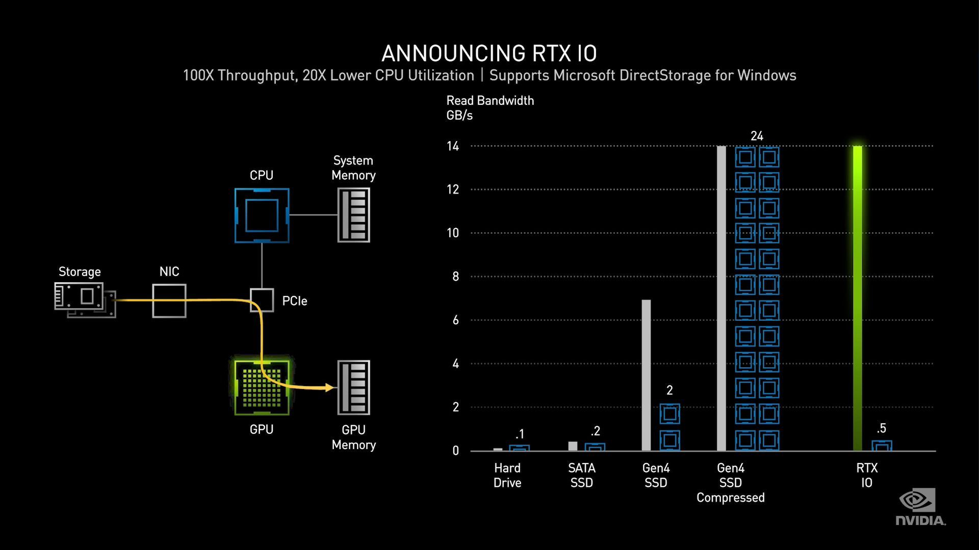
Finally, with the launch of the RTX 30 series, NVIDIA is also announcing a new suite of I/O features that they’re calling RTX IO. At a high level this appears to be NVIDIA’s implementation of Microsoft’s forthcoming DirectStorage API, which like on the Xbox Series X console where it’s first launching, allows for direct, asynchronous asset streaming from storage to the GPU. By bypassing the CPU for much of this work, DirectStorage (and by extension RTX IO) can improve both I/O latency and throughput to the GPU by letting the GPU more directly fetch the resources it needs.
The most significant innovation here, besides Microsoft providing a standardized API for the technology, is that Ampere GPUs are capable of directly decompressing assets. Game assets are frequently compressed for storage purposes – least Flight Simulator 2020 take up even more SSD space – and currently decompressing those assets to something the GPU can use is the job of the CPU. Offloading it from the CPU not only frees it up for other tasks, but ultimately it gets rid of a middleman entirely, which helps to improve asset streaming performance and game load times.
Pragmatically speaking, we already know this technology is coming to the Xbox Series X and PlayStation 5, so this is largely Microsoft and NVIDIA keeping parity with the next-generation consoles. None the less, it does require some real hardware improvements on the GPU end of things to handle all of these I/O requests and to be able to efficiently decompress various types of assets.
Ampere Power Efficiency Improvements: 1.9x? Probably Not
Next to overall video card performance, NVIDIA’s second big technology pillar as part of their presentation was overall power efficiency. With power efficiency being a cornerstone of GPU design – graphics workloads are embarrassingly parallel and GPU performance is capped by total power consumption – power efficiency is a frequent focus across all GPU launches. And for the RTX 30 series launch NVIDIA made sure to give it some attention.
On the whole, NVIDIA is claiming that Ampere offers a 1.9x increase in power efficiency. For a full jump in manufacturing process nodes in the post-Dennard era, this is actually a bit of a surprising claim. It’s far from impossible, mind you, but it’s more than what NVIDIA got out of Turing or Pascal before it.
However digging into NVIDIA’s claims a bit more, this 1.9x claim increasingly looks exaggerated – or at least cherry-picked.
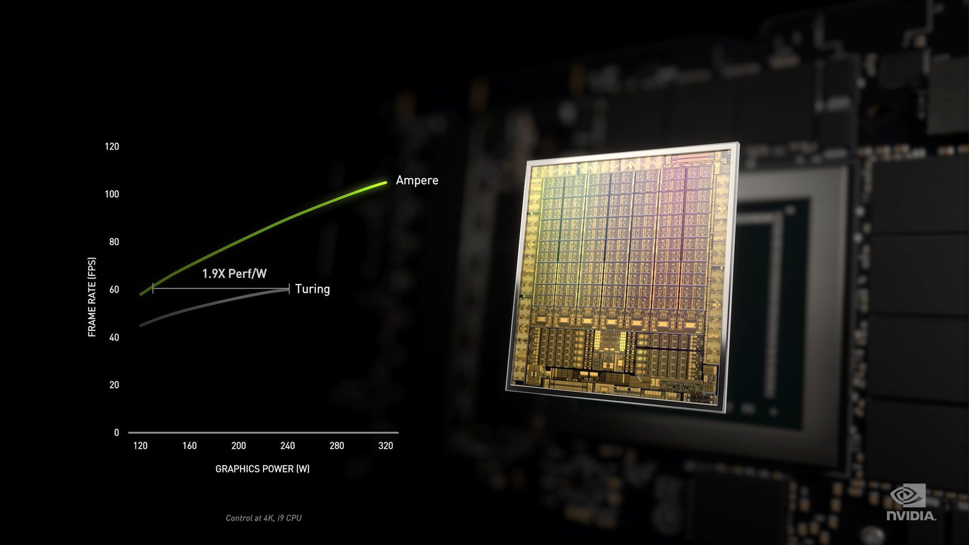
The immediate oddity here is that power efficiency is normally measured at a fixed level of power consumption, not a fixed level of performance. With power consumption of a transistor increasing at roughly the cube of the voltage, a “wider” part like Ampere with more functional blocks can clock itself at a much lower frequency to hit the same overall performance as Turing. In essence, this graph is comparing Turing at its worst to Ampere at its best, asking “what would it be like if we downclocked Ampere to be as slow as Turing” rather than “how much faster is Ampere than Turing under the same constraints”. In other words, NVIDIA’s graph is not presenting us with an apples-to-apples performance comparison at a specific power draw.
If you actually make a fixed wattage comparison, then Ampere doesn’t look quite as good in NVIDIA’s graph. Whereas Turing hits 60fps at 240W in this example, Ampere’s performance curve has it at roughly 90fps. Which to be sure, this is still a sizable improvement, but it’s only a 50% improvement in performance-per-watt. Ultimately the exact improvement in power efficiency is going to depend on where in the graph you sample, but it’s clear that NVIDIA’s power efficiency improvements with Ampere, as defined by more normal metrics, are not going to be 90% as NVIDIA’s slide claims.
All of which is reflected in the TDP ratings of the new RTX 30 series cards. The RTX 3090 draws a whopping 350 watts of power, and even the RTX 3080 pulls 320W. If we take NVIDIA’s performance claims at their word – that RTX 3080 offers up to 100% more performance than RTX 2080 – then that comes with a 49% hike in power consumption, for an effective increase in performance-per-watt of just 34%. And the comparison for the RTX 3090 is even harsher, with NVIDIA claiming a 50% performance increase for a 25% increase in power consumption, for a net power efficiency gain of just 20%.
Ultimately, it’s clear that a good chunk of NVIDIA’s performance gains for the Ampere generation are going to come from higher power consumption limits. With 28B transistors the cards are going to be fast, but it’s going to take more power than ever before to light them all up.
GDDR6X: Cooking With PAM
Outside of the core GPU architecture itself, GA102 also introduces support for another new memory type: GDDR6X. A Micron and NVIDIA developed evolution of GDDR6, GDDR6X is designed to allow for higher memory bus speeds (and thus more memory bandwidth) by using multi-level signaling on the memory bus. By employing this strategy, NVIDIA and Micron can continue to push the envelope on cost-effective discrete memory technologies, and thus continue to feed the beast that is NVIDIA’s latest generation of GPUs. This marks the third memory technology in as many generations for NVIDIA, having gone from GDDR5X to GDDR6 to GDDR6X
Micron accidentally spilt the beans on the subject last month, when they posted some early technical documents on the technology. By employing Pulse Amplitude Modulation-4 (PAM4), GDDR6X is able to transmit one of four different symbols per clock, in essence moving two bits per clock instead of the usual one bit per clock. For the sake of brevity I won’t completely rehash that discussion, but I’ll go over the highlights.
At a very high level, what PAM4 does versus NRZ (binary coding) is to take a page from the MLC NAND playbook, and double the number of electrical states a single cell (or in this case, transmission) will hold. Rather than traditional 0/1 high/low signaling, PAM4 uses 4 signal levels, so that a signal can encode for four possible two-bit patterns: 00/01/10/11. This allows PAM4 to carry twice as much data as NRZ without having to double the transmission bandwidth, which would have presented an even greater challenge.
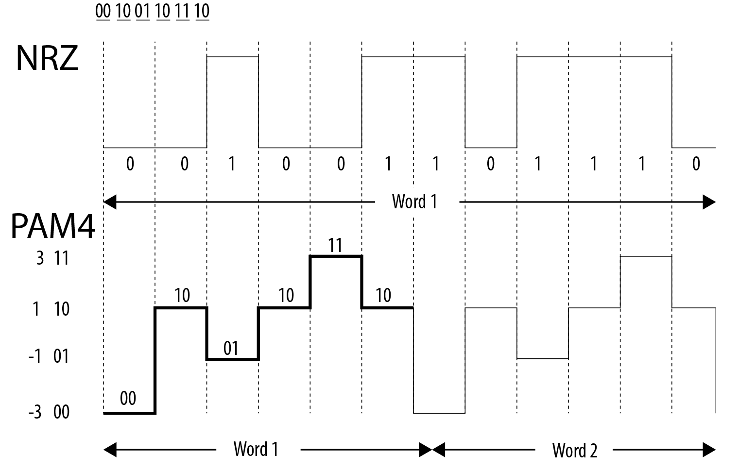
NRZ vs. PAM4 (Base Diagram Courtesy Intel)
PAM4 in turn requires more complex memory controllers and memory devices to handle the multiple signal states, but it also backs off on the memory bus frequency, simplifying some other aspects. Perhaps most importantly of which for NVIDIA at this point is that it’s more power efficient, taking around 15% less power per bit of bandwidth. To be sure, total DRAM power consumption is still up because that’s more than offset by bandwidth gains, but every joule saved on DRAM is another joule that can be dedicated to the GPU instead.
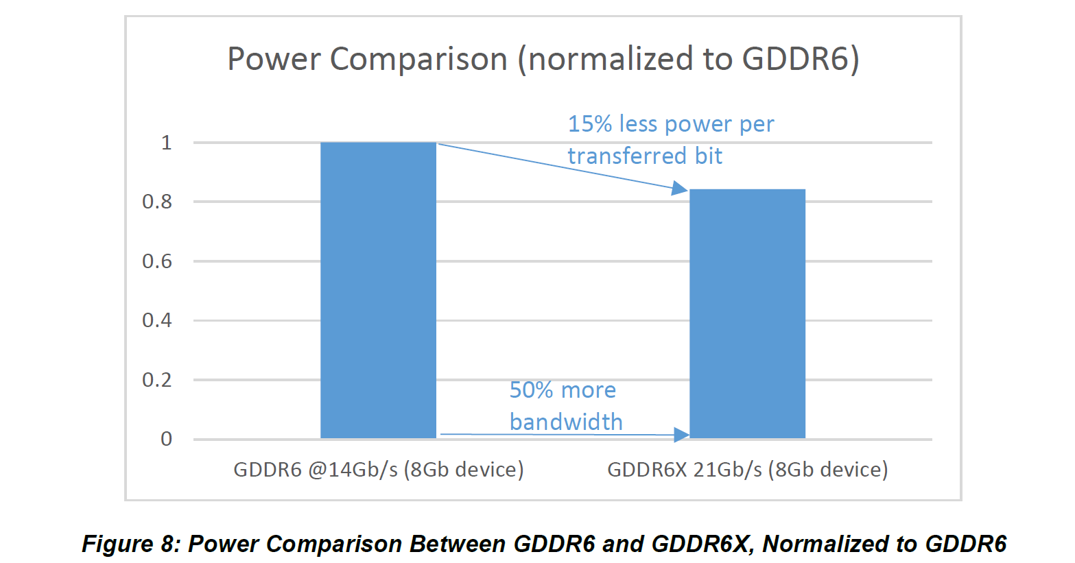
According to Micron’s documents, the company designed the first generation of their GDDR6X to go to 21Gbps; however NVIDIA is keeping things a bit more conservative and stopping at 19.5Gbps for the RTX 3090, and 19Gbps for the RTX 3080. Even at those speeds, that’s still a 36%-39% increase in memory bandwidth over the previous generation of cards, assuming identically-sized memory buses. Overall this kind of progress remains the exception to the norm; historically speaking we typically don’t see memory bandwidth gains quite this large over successive generations. But with many more SMs to feed, I can only imagine that NVIDIA’s product teams are glad to have it.
GDDR6X does come with one somewhat immediate drawback however: capacity. While Micron has plans for 16Gbit chips in the future, to start things out today they’re only making 8Gbit chips in the future. This is the same density as the memory chips on NVIDIA’s RTX 20 series cards, and their GTX 1000 series cards for that matter. So there are no “free” memory capacity upgrades, at least for these initial cards. RTX 3080 only gets 10GB of VRAM versus 8GB on RTX 2080, and that’s by virtue of using a larger 320-bit memory bus (which is to say, 10 chips instead of 8). Meanwhile RTX 3090 gets 24GB of VRAM, but only by using 12 pairs of chips in clamshell mode on a 384-bit memory bus, making for more than twice as many memory chips as on RTX 2080 Ti.
HDMI 2.1 & AV1 Are In, VirtualLink Is Out
On the display I/O front, Ampere and the new GeForce RTX 30 series cards make a couple of notable changes as well. The most important of which is that, at long last, HDMI 2.1 support has arrived. Already shipping in TVs (and set to ship in this year’s consoles), HDMI 2.1 brings a few features to the table, most notably support for much greater cable bandwidth. An HDMI 2.1 cable can carry up to 48Gbps of data – more than 2.6x as much as HDMI 2.0 – allowing for much higher display resolutions and refresh rates, such as 8K TVs or 4K displays running at upwards of 165Hz. This significant jump in bandwidth even puts HDMI ahead of DisplayPort, at least for now; DisplayPort 1.4 only offers around 66% the bandwidth, and while DisplayPort 2.0 will eventually beat that, it would seem that Ampere is just a bit too early for that technology.
With all of that said, I’m still waiting on confirmation from NVIDIA about whether they support a full 48Gbps signaling rate with their new GeForce cards. Some HDMI 2.1 TVs have been shipping with support for lower data rates, so it’s not inconceivable that NVIDIA may do the same here.
HDMI 2.1’s other marquee feature from a gaming standpoint is support for variable refresh rates over HDMI. However this feature is not exclusive to HDMI 2.1, and indeed has already been backported to NVIDIA’s RTX 20 cards, so while support for it is going to be more useful here with the greater cable bandwidth, it technically is not a new feature to NVIDIA’s cards.
Meanwhile VirtualLink ports, which were introduced on the RTX 20 series of cards, are on their way out. The industry’s attempt to build a port combing video, data, and power in a single cable for VR headsets has fizzled, and none of the big 3 headset manufacturers (Oculus, HTC, Valve) used the port. So you will not find the port returning on RTX 30 series cards.
Finally, while we’re on the subject of video, NVIDIA has also confirmed that the new Ampere GPUs include an updated version of their NVDEC video decode block. Bringing the block up to what NVIDIA calls Gen 5, the chipmaker has added decode support for the new AV1 video codec.
The up-and-coming royalty free codec is widely expected to become the de facto successor to H.264/AVC, as while HEVC has been on the market for a number of years (and is already supported in all recent GPUs), the madcap royalty situation around the codec has discouraged its adoption. By contrast, AV1 should deliver similar or slightly better quality than HEVC without royalties for its use in distribution, which makes it a lot more palatable to content vendors. The one downside to AV1 thus far is that it’s pretty CPU heavy, which makes hardware decode support important, even in high-end desktops, in order to avoid tying up the CPU and to ensure smooth, glitch-free playback.
NVIDIA hasn’t gone too much into details here on what their AV1 support entails, but a separate blog post mentions 10-bit color support and 8K decoding, so it sounds like NVIDIA has its bases covered.
Meanwhile, there is no mention of further improvements to the company’s NVENC block. That was most recently revised for the Turing launch, improving the scope of NVIDIA’s HEVC encoding capabilities and overall HEVC & H.264 image quality. Otherwise, we’re still a generation too early for hardware AV1 encoding, as some of the unique properties of that codec are making hardware encoding a tougher nut to crack.


410 Comments
View All Comments
Zingam - Wednesday, September 2, 2020 - link
How come 3090/3080 have the same amount of transistors but totally different CUDA cores count?Why is that discrepancy? Where did the 3080's transistors go?
Ej24 - Wednesday, September 2, 2020 - link
They're physically the same die. The number of transistors is identical. Many are dedicated to pcie communication, memory controller, etc. Not just cuda cores. The number of fully functioning transistors may ultimately be different though. Thus less functioning Cuda cores.Im curious why the Nvidia Cuda core numbers are exactly double what the AIBs have been saying..? That's strange.
eddman - Wednesday, September 2, 2020 - link
Nowhere, they are just disabled. They both use the same chip, so the transistor count is the same.Zingam - Friday, September 4, 2020 - link
I would think they wouldn't count the disabled transistors. That's an interesting way to boost your numbers for marketing.Thanx for the answers!
eddman - Friday, September 4, 2020 - link
It has always been this way, for both nvidia and AMD/ATI.Olternaut - Wednesday, September 2, 2020 - link
Can you please explain to me how the $1500 price of the 3090, the Titan replacement, being almost $100 L E S S than the last Titan, is somehow reaching new heights in pricing as you put it? You are confusing me.Olternaut - Wednesday, September 2, 2020 - link
I meant to say $1000 less. Why doesn't your site have an edit button?Luminar - Wednesday, September 2, 2020 - link
Why can't you proofread your comment before smashing the submit button?Spunjji - Wednesday, September 2, 2020 - link
It's okay, your comment was wild either way, something which will be conclusively demonstrated when they eventually release a 3000-series Titan.DanielLW - Wednesday, September 2, 2020 - link
Scarcity. Perhaps 80% of dies end up with enough working CUDA cores to be a 3080. 15% have enough working cores to be a 3090. And maybe 5% have enough to be a (speculating) 30 series Titan.