TSMC Details 3nm Process Technology: Full Node Scaling for 2H22 Volume Production
by Andrei Frumusanu on August 24, 2020 3:30 PM EST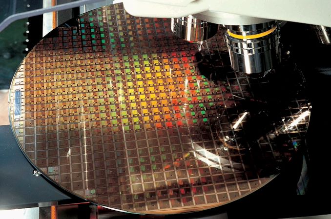
At TSMC’s annual Technology Symposium, the Taiwanese semiconductor manufacturer detailed characteristics of its future 3nm process node as well as laying out a roadmap for 5nm successors in the form of N5P and N4 process nodes.
Starting off with TSMC’s upcoming N5 process node which represents its 2nd generation deep-ultraviolet (DUV) and extreme-ultraviolet (EUV) process node after the rarely used N7+ node (Used by the Kirin 990 SoC for example). TSMC has been in mass production for several months now as we’re expecting silicon shipping to customers at this moment with consumer products shipping this year – Apple’s next-generation SoCs being the likely first candidates for the node.
TSMC details that N5 currently is progressing with defect densities one quarter ahead of N7, with the new node having better yields at the time of mass production than both their predecessor major nodes N7 and N10, with a projected defect density that’s supposed to continue to improve past the historic trends of the last two generations.
The foundry is preparing a new N5P node that’s based on the current N5 process that extends its performance and power efficiency with a 5% speed gain and a 10% power reduction.
Beyond N5P, TSMC is also introducing the N4 node that represents a further evolution from the N5 process, employing further EUV layers to reduce masks, with minimal migration work required by chip designers. We’ll be seeing N4 risk production start in 4Q21 for volume production later in 2022.
Today’s biggest news was TSMC’s disclosure on their next big leap past the N5 process node generation family, which is the 3nm N3 node. We’ve heard that TSMC had been working on defining the node back last year with progress going well.
Contrary to Samsung’s 3nm process node which makes use of GAA (Gate-all-around) transistor structures, TSMC will instead be sticking with FinFET transistors and relying on “innovative features” to enable them to achieve the full-node scaling that N3 promises to bring.
| Advertised PPA Improvements of New Process Technologies Data announced during conference calls, events, press briefings and press releases |
||||||||
| TSMC | ||||||||
| N7 vs 16FF+ |
N7 vs N10 |
N7P vs N7 |
N7+ vs N7 |
N5 vs N7 |
N5P vs N5 |
N3 vs N5 |
||
| Power | -60% | <-40% | -10% | -15% | -30% | -10% | -25-30% | |
| Performance | +30% | ? | +7% | +10% | +15% | +5% | +10-15% | |
| Logic Area Reduction % (Density) |
70% |
>37% |
- |
~17% |
0.55x -45% (1.8x) |
- |
0.58x -42% (1.7x) |
|
| Volume Manufacturing |
Q2 2019 |
Q2 2020 | 2021 | H2 2022 | ||||
Compared to it’s N5 node, N3 promises to improve performance by 10-15% at the same power levels, or reduce power by 25-30% at the same transistor speeds. Furthermore, TSMC promises a logic area density improvement of 1.7x, meaning that we’ll see a 0.58x scaling factor between N5 and N3 logic. This aggressive shrink doesn’t directly translate to all structures, as SRAM density is disclosed at only getting a 20% improvement which would mean a 0.8x scaling factor, and analog structures scaling even worse at 1.1x the density.
Modern chip designs are very SRAM-heavy with a rule-of-thumb ratio of 70/30 SRAM to logic ratio, so on a chip level the expected die shrink would only be ~26% or less.
N3 is planned to enter risk production in 2021 and enter volume production in 2H22. TSMC’s disclosed process characteristics on N3 would track closely with Samsung’s disclosures on 3GAE in terms of power and performance, but would lead more considerably in terms of density.
We’ll be posting more detailed content from TSMC’s Technology Symposium in due course, so please stay tuned for more information and updates.
Related Reading:
- TSMC: N7+ EUV Process Technology in High Volume, 6nm (N6) Coming Soon
- TSMC Announces Performance-Enhanced 7nm & 5nm Process Technologies
- TSMC: Most 7nm Clients Will Transition to 6nm
- TSMC Reveals 6 nm Process Technology: 7 nm with Higher Transistor Density
- TSMC’s 5nm EUV Making Progress: PDK, DRM, EDA Tools, 3rd Party IP Ready
- TSMC: 7nm Now Biggest Share of Revenue
- TSMC: First 7nm EUV Chips Taped Out, 5nm Risk Production in Q2 2019
- TSMC Details 5 nm Process Tech: Aggressive Scaling, But Thin Power and Performance Gains


58 Comments
View All Comments
nandnandnand - Monday, August 24, 2020 - link
We haven't even seen monolithic 3D yet. There's more performance per dollar/Watt to be realized, and that doesn't help SaaS. There will be an enthusiast/DIY market in 2025+. Probably with x86, ARM, and RISC-V options. The market won't exist by 2050 because everyone will be dead.Spunjji - Wednesday, August 26, 2020 - link
Nailed it on future projections.brucethemoose - Monday, August 24, 2020 - link
In the US, its not just node scaling thats slowing though. Stuff-as-a-service requires exponential internet access as well.Line-of-sight mmWave and such not going to work with everyone moving out of cities now, and unless the FCC does something radical, we're running out longer range, longer wavelength bands to comandeer.
Meanwhile, landline ISPs have seemingly captured regulatory bodies, and stalled.
defferoo - Monday, August 24, 2020 - link
There's no way Apple is moving to an OS as a service. They are firmly planted in the edge computing camp. Going over a network for everything is a bad user experience from a performance, latency, bandwidth, power consumption, and privacy perspective. Not to mention, the device stops functioning when you lose network? This is literally why they build their own processors, so that nearly everything can be done locally instead of a server.Spunjji - Wednesday, August 26, 2020 - link
Yeah, I was confused by that "inference" too. Apple have consciously been at the forefront of pushing CPU and GPU performance in phones for at least half of the last decade. It would be extremely weird for them to have pushed that hard and then suddenly decide not to bother anymore.Tams80 - Tuesday, August 25, 2020 - link
Not so soon. Fast Internet connections are just not there. In urban areas there are just too many users and rural areas are expensive to roll-out to.Unfortunately, I don't think latency will be cared about much, even though there's no real fix for it other an AI prediction. There's just not enough demand for extremely low latency.
nandnandnand - Monday, August 24, 2020 - link
"Modern chip designs are very SRAM-heavy with a rule-of-thumb ratio of 70/30 SRAM to logic ratio, so on a chip level the expected die shrink would only be ~26% or less."How was the SRAM scaling between N7 and N5? N3 might be good enough for a core count doubling in the same area from N7.
Gondalf - Monday, August 24, 2020 - link
Definitively it is not a full node scaling, combining logic with sram.....this is an half node, nothing more. Obviously outside very low power SOC devices the shrink in logic will be a lot lower than their 0.58X.In summary these are nodes aimed for phone makers and NOT for Pc/server makers.
Right now N5 is a step behind in comparison to the goodies of N7 (the advantages are very questionable. sure not at the level of N7 over 12/16nm or 10nm), that will remain the real golden node for TSMC.
Both N5 and N3 are a little delusion under many parameters. The lack of sram scaling will be an huge issue for cpu and GPU makers.
But TSMC was fair saying 7nm will remain the right horse for some years in future.
eek2121 - Monday, August 24, 2020 - link
It doesn’t matter, they are beating everyone else. The node name is just a name. Nothing more.name99 - Monday, August 24, 2020 - link
Oh JFC!You do realize that no-one on earth cares about your "full node scaling" anymore except a few shills in Intel marketing?
People like you have been beating the "not a full node scaling" drum since TSMC 20nm; how's that working out for you?