Intel Moving to Chiplets: ‘Client 2.0’ for 7nm
by Dr. Ian Cutress on August 21, 2020 5:00 PM EST- Posted in
- CPUs
- Intel
- GPUs
- Client
- Intel Arch Day 2020
- Client 2.0
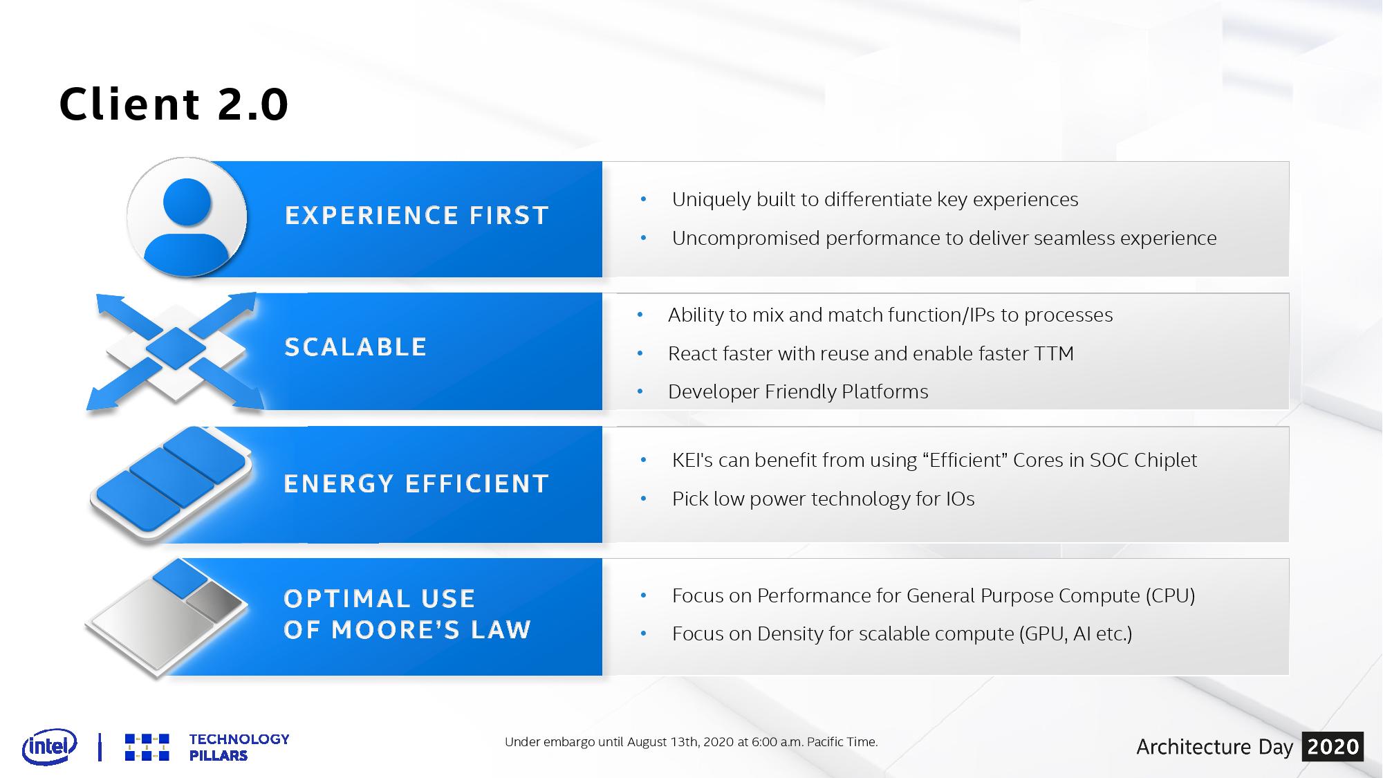
One of the more esoteric elements of Intel’s Architecture Day 2020 came very near the end, where Intel spent a few minutes discussing what it believes is the future of some of its products. Brijesh Tripathi, VP and CTO of Intel’s Client Computing group, laid out a vision about the future of its client products in the 2024+ future timeframe. Centered around Intel’s 7+ manufacturing process, the goal was to enable ‘Client 2.0’ – a new way to deliver and enable immersive experiences through a more optimized silicon development strategy.
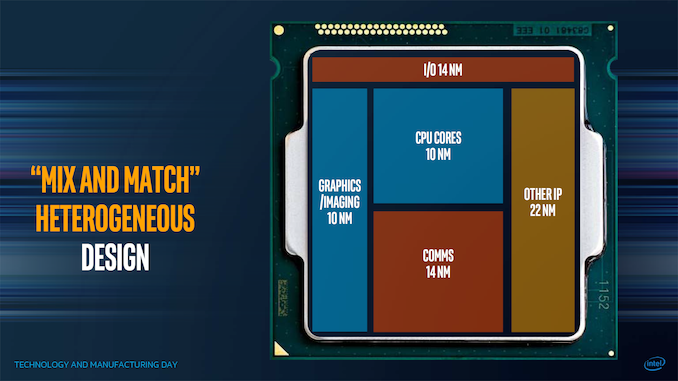
Chiplets aren’t new, especially with recent launches from Intel’s competitors, and as we move into more complex process node development, the era of chiplets enables faster time-to-market as well as better binning and yields for a given product. The key is enabling how those chiplets fit together, and at which points it makes sense to mix and match the relevant ones. Intel has spoken about this before in a more generalized context, at its Technology and Manufacturing Day 2017, as shown in the carousel image at the top.
The goal here is to mix and match which process nodes work best for different parts of the chip. Intel seems set to realize this vision starting with its 7nm platform. At Architecture Day 2020, Brijesh Tripathi showed this slide:
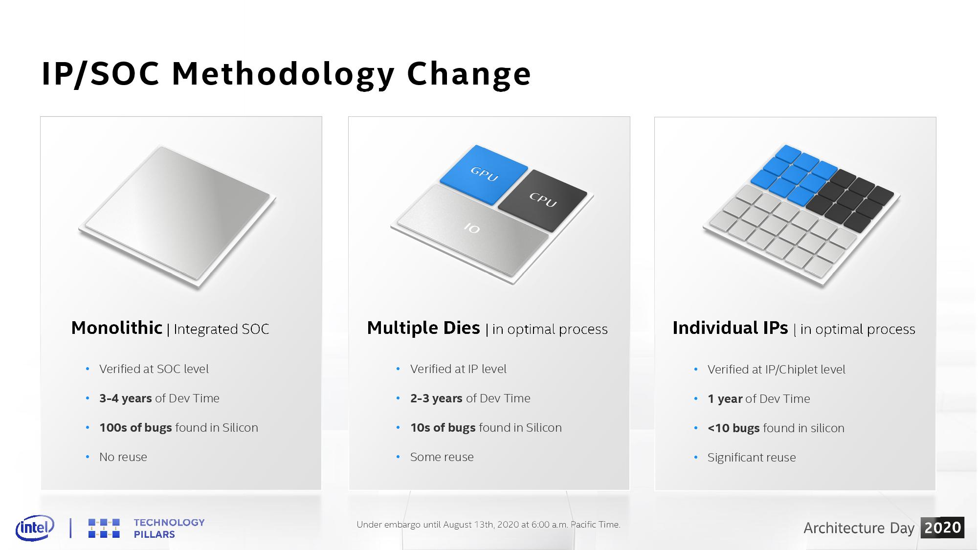
On the left is a typical chip design – monolithic with everything it requires. For Intel’s leading edge products, these take 3-4 years to develop, and bugs are found in silicon by both Intel initially and then later by Intel’s partners as they can ramp up the silicon-on time by a a few orders of magnitude.
In the middle is a basic chiplet layout, similar to that slide from 2017, where different functions of the die are split into their own modules. Assuming a consistent interconnect, there are some reuse of the silicon elements, such as AMD using the same core compute dies in client and server. For some semiconductor companies (except Intel), this is where we are.
On the right is where Intel sees its future. Instead of having a single digit number of chiplets in a product, it envisions a world where each IP can be split into multiple chiplets, enabling products to be built with different configurations of what works for the market. In this instance, a chiplet might be a PCIe 4.0 x16 link – if the product needs more, it simply adds in more of these chiplets. Same with memory channels, cores, media accelerators, AI accelerators, Ray Tracing engines, crypto accelerators, graphics, or even as far down as SRAM and caching blocks. The idea is that each IP can be split and then scaled. This means that the chiplets are tiny, can be built relatively quickly, and bugs should be ironed out very quickly.

In this diagram, we are treated to Intel’s long term vision for the client – a base interposer with an in-package memory (something like an L3 or L4) that can act as the main SRAM cache for the whole die, and then on top of this we get 24 different chiplets. Chiplets can be graphics, cores, AI, Media, IO, or anything else, but they can be mixed and matched based on what is needed. A content creator might want a balance between some good graphics acceleration and compute, while a gamer might want to focus purely on the graphics. A corporate client or workstation might need less graphics and more for compute and AI, whereas a mobile version of the chip will be heavily invested in IO.
As always, there is some trade-off between chiplet size and complexity of actually putting them together in a multi-die arrangement. Any communications between chiplets costs more power than a monolithic interpretation, and usually offer higher latency. Thermals have to be managed as well, and so sometimes those chiplets are limited by what thermal properties are available. Multi-die arrangements also cause headaches for mobile devices, where z-height is critical. However, the benefits afforded from using the right process at the right time for the right product are big, as it helps provide both performance and power at the best possible cost. It also gives the opportunity to bring in 3rd party IP quickly if something amazing hits the scene.
The only downside here is that Intel hasn’t spoken much about the glue that binds it all together. Chiplet strategies rely on complex high-speed interconnect protocols, custom or otherwise. Current uses of Intel’s die-to-die connectivity are either simply memory protocols or FPGA fabric extensions – the big ones for server CPUs like UPI aren’t necessarily up to the task. CXL could be the future here, however current CXL is built upon PCIe, which means a complex CXL/PCIe controller for every chiplet which will likely get power hungry fast.
Intel has stated that they are inventing new packaging technology and new levels of connectivity to act between the silicon - there is no disclosure on the protocols at this time, however Intel acknowledges that to get to this level of scale it will have to go beyond what the company has today, and that will require creating standards and innovation in this area. The goal is to create and support standards, and the first incarnation will have some standardization built in. Intel states that this is a method of extreme disaggregation, and to note that not everything that is connected has to be high bandwidth (such as USB) or a coherent interconnect - Intel sees the goal involving a handful of protocols throughout the spectrum.
There’s also the developer market, which might be used to a more homogeneous implementation of resources in any given product. Without careful planning, and relevant coding, there is the potential for certain chiplet configurations to fall over if the developer was expecting a certain ratio of compute to graphics, for example. This isn’t something that OneAPI could easily fix.
These are all issues that Intel will have to address, although they have a few years until this comes to fruition. We were told that the internal name is Client 2.0, although it will likely have more marketing dressing added as Intel starts talking about it in more detail.
Related Reading
- Intel's Interconnected Future: Combining Chiplets, EMIB, and Foveros
- Intel 7nm Delayed By 6 Months; Company to Take “Pragmatic” Approach in Using Third-Party Fabs
- The Intel Lakefield Deep Dive: Everything To Know About the First x86 Hybrid CPU
- Intel to use Nanowire/Nanoribbon Transistors in Volume ‘in Five Years’


67 Comments
View All Comments
Spunjji - Monday, August 24, 2020 - link
Comment-and-run, no less. No response, no retraction. It's getting increasingly difficult to tell whether stuff like this is just people getting up in their feelings, or a group purposefully disrupting the comments to provide an illusion of commenters rejecting a reviewer's "bias" :/at_least_3db - Monday, August 24, 2020 - link
The comment was in part a slap back to intel's comment about AMD's "glued together solution " a few years back. It was meant as an insult to AMD, but how the tables have turned.Secondly, as other commented, there is a difference between the fabrication technology, and the protocol. See AMD infinity fabric for comparison of what we want.
Quantumz0d - Friday, August 21, 2020 - link
All show, this time they got someone to make new BS slides to look fresh. And got some new shiny trash to show off. Dafaq is that gamer and creator bs chiplet design, on top with AI, what AI are you going to stuff in Intel, that Intel HW scheduler with Big Little garbage to make up for the big core SMT performance ?Man they are really out of ideas, Ian's aspect of "which glue" is perfectly apt here, we know AMD processors have limitations around the Infinity Fabric and how IMC works alongside the cache and other IP on the whole Ryzen chip and how AMD improving it as they learn. With Intel none of them shown and where are the products, copying AMD is what they are doing now, chiplet design and now this, what else, wait for 7nm ? Xe was outsourced to TSMC, if it fails then Raja can retire.
Let's see what Ice Lake delivers first on Xeon platform and how RKL wants to be relevant with their 5.0GHz clocks but lower core count due to non scalable ring bus on power hungry 14nm++ design, 14nm++ is a technology feat for sure, competing with AMD parts on 7nm but it's very old now, SMT performance is already taking a hit...
Lord of the Bored - Friday, August 21, 2020 - link
"copying AMD is what they are doing now"Hey, it kept them relevant in the AMD64 days and bought them enough time to engineer their way out of the Pentium 4-shaped hole they'd dug. Maybe it can save them this time too.
nathanddrews - Saturday, August 22, 2020 - link
Hey, if people can get AMD's class-leading and affordable high core count and next gen features alongside Intel's class-leading single-threaded frequencies, that would officially be the best CPU ever made. So yeah, it would certainly *save* Intel.FunBunny2 - Friday, August 21, 2020 - link
this talk about chiplets, Intel AMD et al reminds me of my first RS/6000 install. 5 chips, I think... well, the wiki says that the multi-chip versions from the early 90s (when I was involved) had at least 6 chips."The lower cost RIOS.9 configuration had 8 discrete chips—an instruction cache chip, fixed-point chip, floating-point chip, 2 data cache chips, storage control chip, input/output chip, and a clock chip. "
the wiki
kinda the same idea
brucethemoose - Friday, August 21, 2020 - link
Yep, its kinda back to the future.vFunct - Saturday, August 22, 2020 - link
And then it'll all go back to monolithic chips for the generation after this, perhaps through wafer-scale integration like we're seeing with some designs..Alexvrb - Sunday, August 23, 2020 - link
That's silly. Do you have any idea how expensive a wafer is? If they go monolithic again, it will be after they run out of new process nodes to design for. In the meantime, they're planning on doing what AMD is already doing - chiplets. It lets you tweak parts of the whole without a complete redesign, and it lets you mix and match processes based on what you have ready - you can use what is best for a given design, cost, etc.In fact, if you look at their fancy pictures, Intel is thinking of taking it a step further. Which, as others have said, will be very challenging. The "fabric" to make it all work together as one is a major challenge. AMD has spent a lot of time getting it right, even without subdividing their chiplets as Intel is discussing. Further breaking those components up multiplies the challenge. AMD hasn't even released a chiplet based APU (yet), mainly due to how much power it would consume - Renoir made huge power gains, they would have burned all that up in fabric power if they had CPU and GPU chiplets instead of monolithic. It's why they started with chiplets on the desktop and up.
Anyway, we'll see, I'm sure future fabric designs will enable ever-increasing flexibility. Intel has a lot of resources to throw at the problem, and AMD has a lot of experience already. So it should be fascinating to see what they both cook up in the coming years.
JayNor - Wednesday, October 7, 2020 - link
Intel's heterogeneous accelerator solutions using CXL are claimed to be simpler than, for example, requiring UPI or IF on all the accelerators.It isn't clear to me that CXL would imply greater power, since the biased cache coherency is intended to reduce the traffic between CPU and accelerator.
https://www.nextplatform.com/2019/09/18/eating-the...