The Intel Xe-LP GPU Architecture Deep Dive: Building Up The Next Generation
by Ryan Smith on August 13, 2020 9:00 AM EST- Posted in
- GPUs
- Intel
- Tiger Lake
- Xe
- Xe-LP
- DG1
- Intel Arch Day 2020
- SG1
Xe-LP Execution Units: It Takes Two
Diving down a level deeper, we have the smallest thread-level building block of the Xe-LP GPU architecture, the venerable Execution Unit. Intel has tweaked these a few times over the years, and for Xe-LP they are getting tweaked once again.
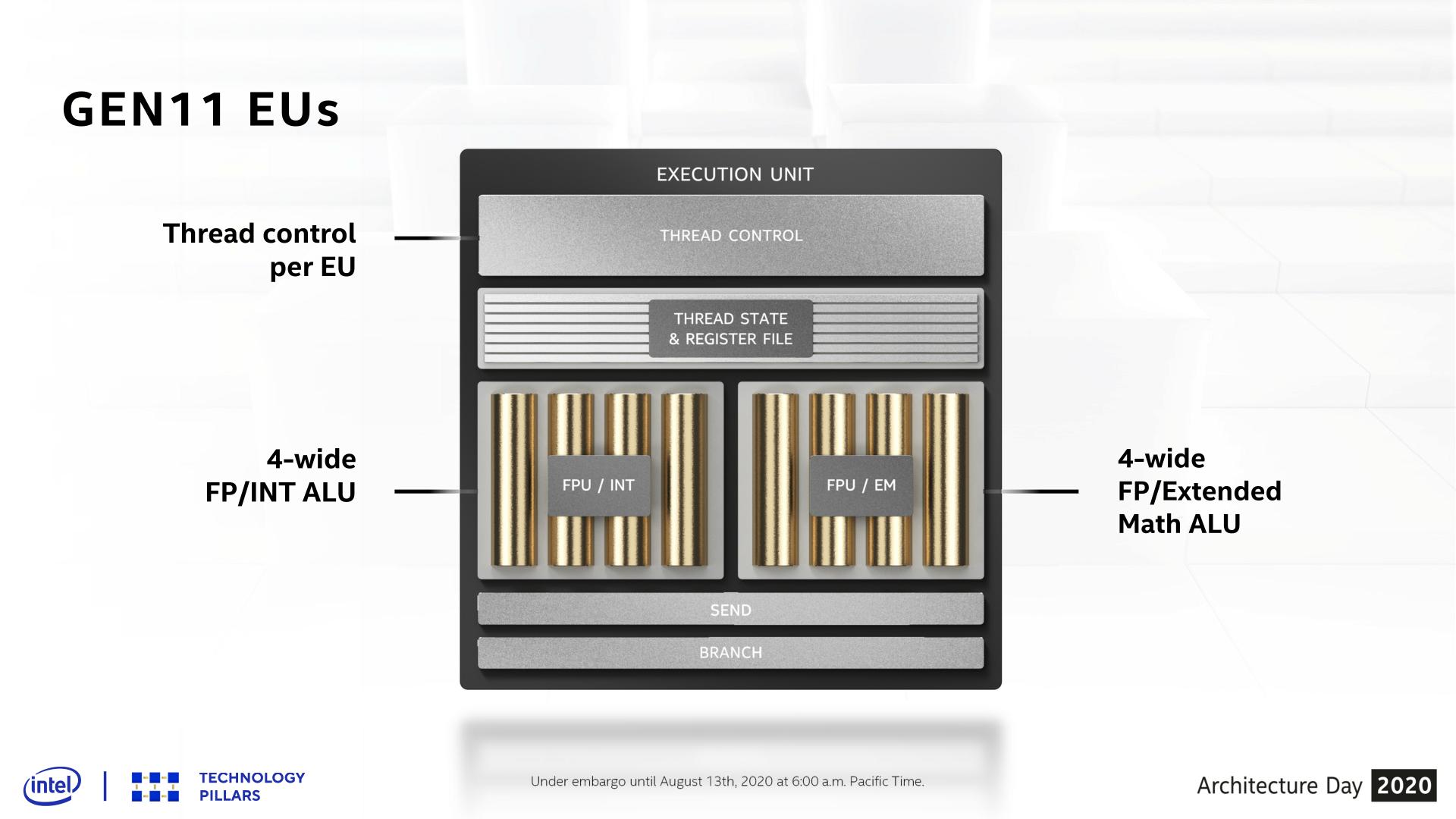
As a quick refresher, as of Intel’s Gen11 GPU architecture, an EU is comprised of a single thread control unit and two sets of 4-wide SIMDs. One block handles floating point and integer math, while the other block can handle floating point and special functions, which Intel refers to as “extended math”. Despite this, Gen11’s smallest wavefront width is 8 threads wide (SIMD8), so it can take multiple clock cycles to execute a single wavefront, with Intel interleaving multiple wavefronts as a form of latency hiding.
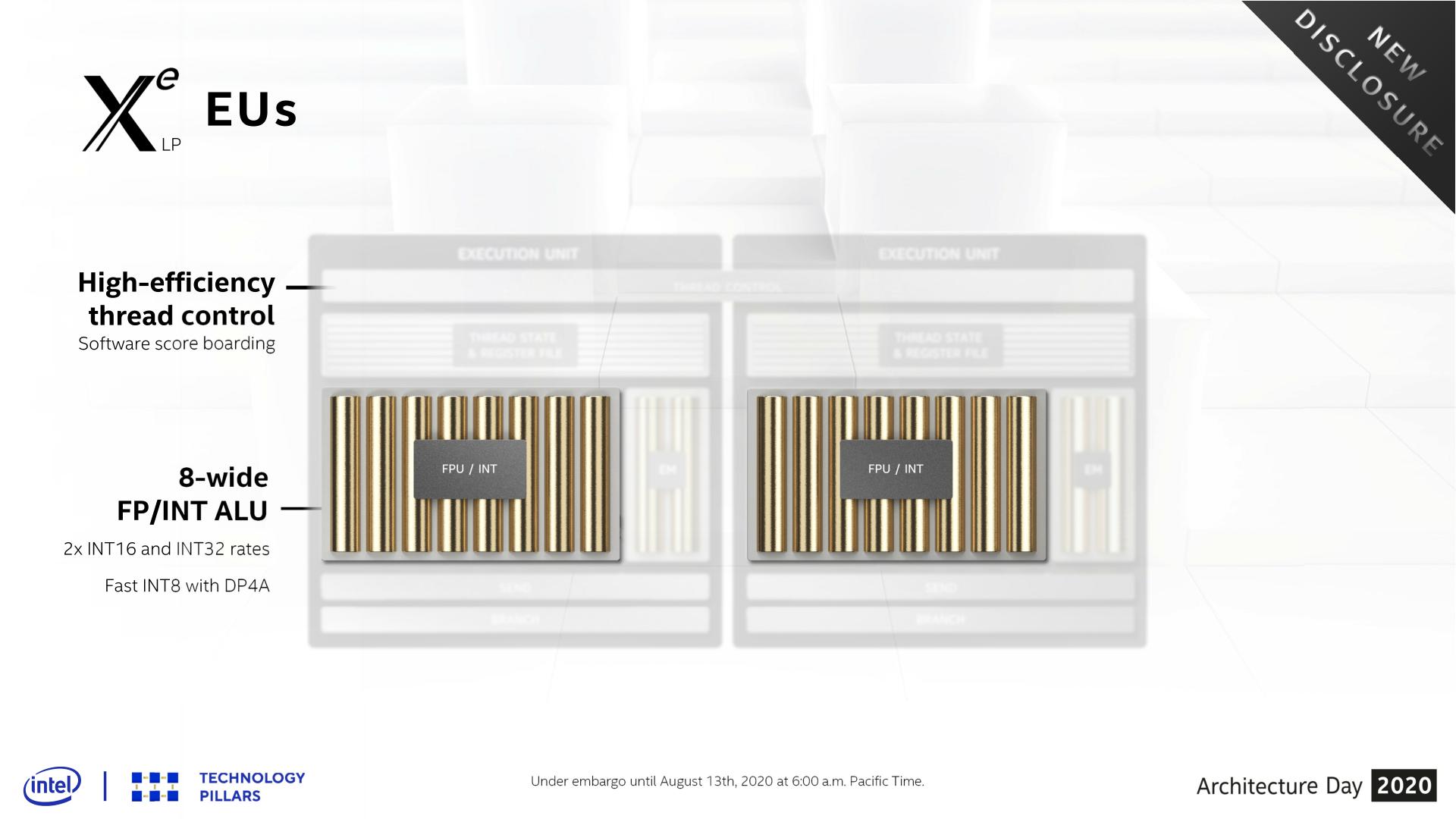
Xe-LP, meanwhile, brings several important changes to the design of the EUs. First and foremost, a single EU is no longer a stand-alone block; instead two EUs now share a single thread control unit. As a result, a thread control unit now gets the combined resource of two EUs to spread work over, instead of the one. And while the SIMD arrays themselves have also changed – further complicating matters – the impact here is that there are now fewer thread control units in a GPU, which should reduce the number of wavefronts that are in-flight at any given moment.
In fact there’s an argument to be had whether calling these dual EU setups two EUs is even the most accurate way to describe them; it might be better to instead bundle them together as a single fat EU, since neither half is truly independent. But absent further low-level details, and what I’m sure is a desire by Intel to be semi-consistent in counting EUs, they are going with 96 thin EUs.
Meanwhile regardless of how you bundle the EUs, there’s also the matter of what’s in the EUs themselves. For Xe-LP, Intel has reorganized the SIMD blocks. Gone are the pair of feature-differentiated SIMD4 blocks in favor of a SIMD8 block and a SIMD2 block. The larger SIMD8 essentially combines all of the floating point and integer ALUs that previously were split between Gen11’s two SIMD4 blocks, and makes a single SIMD8 out of them. The net result is that the number of FPU ALUs hasn’t changed – it’s still 8 ALUs per EU – however the number of pipes that can process integers has changed from 4 to 8. Meanwhile, although not made clear in Intel's slides, the number of ALUs that can process extended math is staying constant: Gen11 had two EM-capable pipes, and Xe-LP does as well.
Speaking of which, extended math has now been moved to its own SIMD2, and every EU gets one. This means that executing extended math functions no longer directly blocks the execution of floating point arithmetic, as was the case for Gen11 – the EU doesn’t have to give up FP pipes to do this. Further underscoring this point, the EU can co-issue instructions to both the FP/INT SIMD8 and the EM SIMD2 at the same time, meaning that under at least some circumstances, doing extended math also won’t indirectly block FP/INT arithmetic.
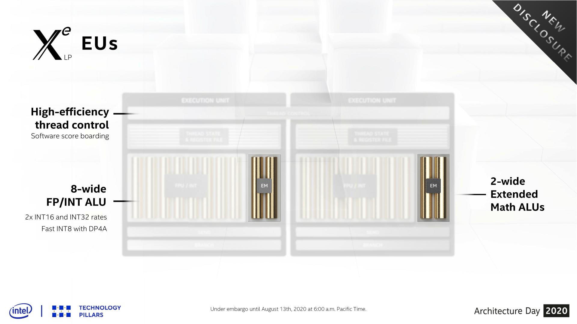
As always with co-issuing, the devil is in the details – at this point it’s not clear to us just what the co-issuing limitations are – but it’s still very likely to be a better fit to the kind of workloads Intel is actually seeing. AMD and NVIDIA also use dedicated EM/SFU units, and in similarly small ratios, all of which seems to work out well for those two companies. So in that respect Intel’s ALU setup is looking a lot more like its contemporary competitors’. And this, I suspect, is also one of the forms of bottleneck optimization that Intel has gone through to get more work out of the same number of FLOPs on Xe-LP.
These ALU changes also impact how wavefronts will move through the GPU. With a SIMD8 being the smallest ALU array for normal arithmetic, Intel’s minimum wavefront size is now the same size as the underlying hardware. This means that Xe-LP no longer needs multiple cycles to execute a single instruction from a wavefront in a single cycle, at least for the smallest wavefront size. In Gen11 Intel also allowed SIMD16 and SIMD32 wavefronts, and I’m waiting on the Xe-LP whitepaper to confirm whether those have been retained – in which case they’d still need multiple cycles – or if Intel is forcing everything to be SIMD8.
It’s worth noting that this change is fairly similar to what AMD did last year with its RDNA (1) architecture, eliminating the multi-cycle execution of a wavefront by increasing their SIMD size and returning their wavefront size. In AMD’s case this was done to help keep their SIMD slots occupied more often and reduce instruction latency, and I wouldn’t be surprised if it’s a similar story for Intel.

A further benefit of this reorganization is that Intel has been able to simplify their thread scheduling hardware overall. As recently as Gen11, Intel was still using hardware score boarding to determine when to run threads and when threads’ data would be ready. But with Xe-LP, score boarding has been moved into software, becoming a responsibility of Intel’s compiler.
While the move to software score boarding means that scheduling has to be determined in advance by the software – and thus becomes static and potentially results in less-than-optimal scheduling – the payoff is that hardware score boarding is fairly expensive from a die area and power standpoint. So moving to software score boarding allows for smaller and more power efficient EUs, which feeds back into Intel’s ability to build a larger number of EUs, and to improve their overall energy efficiency. Overall, this mirrors changes NVIDIA made to their architecture almost a decade ago with Kepler, where they similarly switched to software score boarding to the great benefit of their energy efficiency (and while retaining their high performance).
EU Throughput: By the Numbers
Now that we’ve had a chance to see all the changes made at the EU level, let’s talk about what this means for the actual throughput rates of the EUs.
| Intel GPU Compute Throughput Rates (FMA, Ops/clock/EU) |
||||
| Xe-LP | Gen11 | |||
| FP32 | 16 | 16 | ||
| FP16 | 32 | 32 | ||
| INT32 | 8 | 4 | ||
| INT16 | 32 | 16 | ||
| INT8 | 64 (DP4A) |
N/A | ||
Starting with floating point, things are simple here. Despite the ALU reorganization, the number of FP ALUs per EU is still 8. And as a result, FP throughput per EU remains at 16 FP32 ops/clock and 32 FP16 ops/clock, just like Gen11.
For integer throughput on the other hand, the number of integer-capable ALUs has been doubled from 4 to 8 relative to the Gen11 architecture. As a result, integer throughput has also doubled: Xe-LP can put away 8 INT32 ops or 32 INT16 ops per clock cycle, up from 4 and 16 respectively on Gen11. This does mean, however, that Xe-LP retains Gen11’s unusual INT32 handicap; the INT32 rate is only half the FP32 rate, whereas the INT16 rate is equal to the FP16 rate.
Finally, it’s worth nothing that Xe-LP doesn’t have anything equivalent to a tensor core or other systolic array of ALUs for doing dense math, which has become all the rage for neural networking training an inference. This hardware will be coming to the Xe family in later parts as the Xe Matrix eXtensions (XMX), but for now Xe-LP has to make do with its regular EUs.
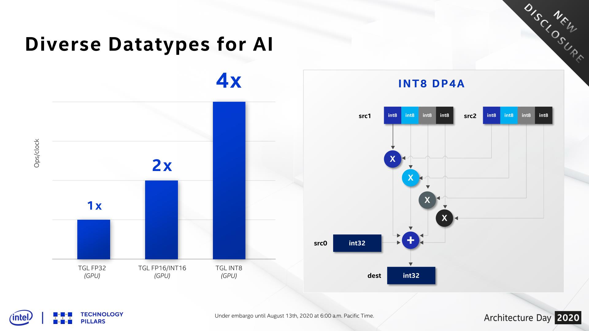
But for that reason, Intel has added one more feature to their EU SIMD: support for INT8 dot products. INT8 has become increasingly popular for neural networking inference over the past few years, and dot products in turn a very common operation in that process. So adding support for INT8 dot products gives Xe-LP a big boost in this form of AI execution. With the DP4A instruction, the INT8 throughput rate can get as high as 64 ops/clock, twice the INT16 rate.


33 Comments
View All Comments
mode_13h - Thursday, August 13, 2020 - link
I can't speak to Direct 3D, but OpenGL talks about work group invocations. I don't believe "threads" is mentioned anywhere in the API.Dolda2000 - Thursday, August 13, 2020 - link
Admittedly I haven't read the whole article yet, but it strikes me how the presentations seems to be comparing the new GPU to the previous GPU, rather than presenting it as a new architecture. Does this confirm that using the "Xe" moniker for this product is just marketing, and that it in fact is an evolution of previous Gen architectures?I mean, I don't mind if that's the case, I just wish they wouldn't overmarket it.
Ryan Smith - Thursday, August 13, 2020 - link
" is an evolution of previous Gen architectures?"It is an evolution of the previous Gen architectures. A major evolution, but an evolution none the less. Not even Intel is going to do a clean sheet design when they have bits and pieces that already work fine.
Dolda2000 - Thursday, August 13, 2020 - link
Certainly, they're not going to create a new clean-slate ALU design just for the sake of it, but it has always been my impression that Xe (at least Xe-HPC) was going to be a more-or-less new architecture. Maybe that has just been my misunderstanding the whole, and Xe-HPC too is going to be fundamentally Gen-based (though I seem to recall that being explicitly denied at some point), but what I was getting at here was that Xe-HPC is going to be the new architecture, and meanwhile this is "merely" an evolution of Gen for which they're just borrowing the product name of their higher-end offering to make it seem like more than what it is.mode_13h - Thursday, August 13, 2020 - link
You should distinguish between the ISA and uArch of the shader cores (EUs) vs. the macro-architecture of the GPU (e.g. buses, memories, caches, fixed-function units, etc.).So, you can have a macro-architecture that's *very* different, even while the ISA is a small evolution and the uArch of the EUs is somewhere in between.
tipoo - Thursday, August 13, 2020 - link
RDNA 1 still has significant GCN bits in it, I'm sure Nvidia does the same a few generations in a row, there's no necessary contention between it being an evolution and it being marked as something substantially new.abufrejoval - Thursday, August 13, 2020 - link
IMHO the overhead of multi GPU rendering with an iGPU and dGPU can't really be offset by the small contribution the iGPU is likely to make to a beefy dGPU.More likely will be dGPU via Thunderbolt 4 and very seamless transitions on docking/undocking and that's good enough.
Too bad that won't work nearly as well with Ryzen notebooks so there again consumer choice goes down the drain somewhat. Not that I believe TB dGPU is a really an attractive market unless prices change dramatically.
mode_13h - Thursday, August 13, 2020 - link
Agreed. I think it would work much better to task the iGPU with other compute tasks that involve less communication bandwidth with the dGPU. Things like physics, AI, audio processing, etc.brucethemoose - Thursday, August 13, 2020 - link
Maybe post processing? Like an Intel version lf ReShade? IIRC the frames have to come back to the IGPU's display block anyway.tipoo - Thursday, August 13, 2020 - link
In this case the IGP would be nearly equivalent to DG1