Intel’s 11th Gen Core Tiger Lake SoC Detailed: SuperFin, Willow Cove and Xe-LP
by Dr. Ian Cutress on August 13, 2020 9:01 AM EST- Posted in
- CPUs
- Intel
- SoCs
- Tiger Lake
- 10+
- Xe-LP
- Willow Cove
- Intel Arch Day 2020
- SuperFin
- 10SF
What is in a Willow Cove Core?
At Intel’s Architecture Day 2018, the company showcased its new CPU core roadmap covering the next several generations of both the high performance cores and the high efficiency cores. Intel updated the slide for the new event.
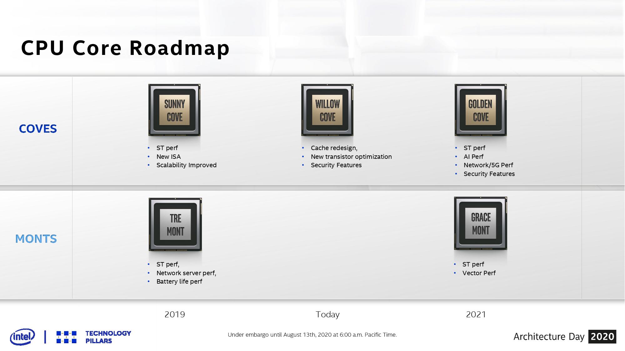
Not so much new has been added, however it is worth covering.
On the top we have the Cove cores, which represent Intel’s high performance designs. It starts with Sunny Cove as the 2019 core, which we can find inside Intel’s Ice Lake and Lakefield processors today. Sunny Cove was set to provide an increase in single threaded performance (we saw 15-20% clock-for-clock), a new set of instructions (VNNI for deep learning), and scalability improvements.
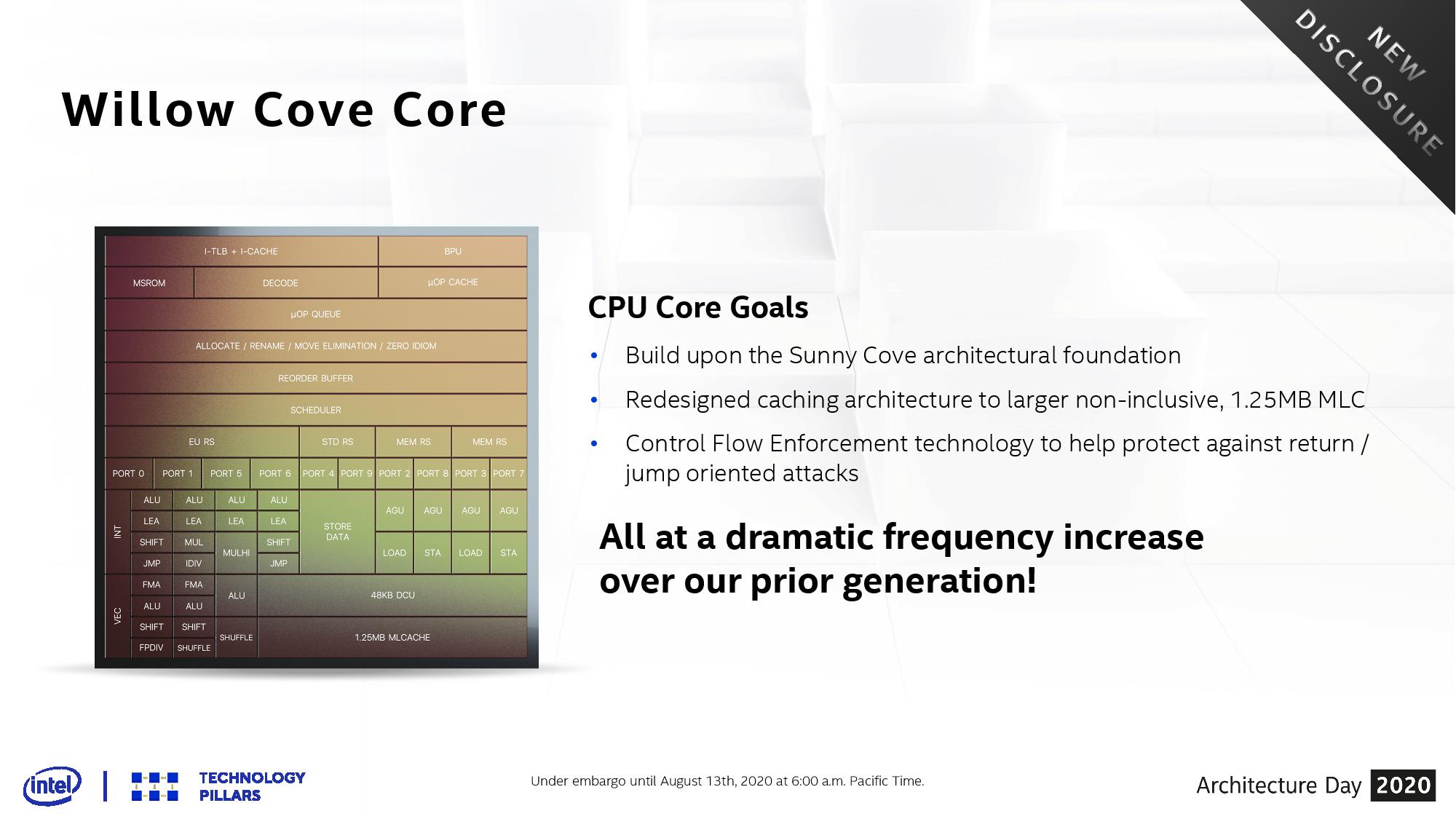
In the middle for the Cove section is Willow Cove, which forms the fundamental compute core for Tiger Lake. On this slide it shows that Willow Cove has a cache redesign (see below), a new transistor optimization (see previous page), and implements new security features.
The 2021 high performance core will be Golden Cove, which Intel states will offer another jump in single threaded performance, more AI performance, and offer performance related to networking and 5G.
Then there’s also some Monts, which are the efficiency-focused Atom cores. We did an analysis of Tremont’s microarchitecture, which you can read here. Gracemont in 2021 will be the Atom core built for Intel’s next generation Hybrid CPU architectures.
Willow Cove: +10-20% Performance Over Sunny Cove
The story of Willow Cove is going to be a bit confusing for a lot of people. It certainly was to me when it was first explained. But I’m going to rip the band-aid off quickly for you, just to get it over and done with.
The microarchitecture of a Willow Cove core is almost identical to that of a Sunny Cove core.
It is almost a copy-paste, but with three key differences that enable a 10-20% performance uplift over Sunny Cove. As it stands, there is no point drawing a diagram to explain the front-end and the back-end of Willow Cove. I suggest you read our deep dive into Sunny Cove, because it’s going to be the same in pretty much all areas. Same branch predictors and decode, same re-order buffers and TLBs, same execution ports, same reservation stations, same load/store capabilities.
Moving the core from Sunny Cove to Willow Cove affords only three differences that need to be highlighted. There is an additional change within the memory subsystem that will be addressed here also.
SuperFin Frequency
First, where most of the performance uplift comes from, is the process node. Moving to 10SF and the new SuperFin transistor has enabled Willow Cove to scale better with respect to voltage and frequency, allowing for better metrics across the board. This means better performance at the same voltage, or the same performance at a lower voltage, compared to Sunny Cove. Where the +10-20% performance comes from is at the high-end. Where Sunny Cove was limited to a peak frequency around 4.0 GHz, Willow Cove appears to promise something more akin to 5.0 GHz.

This is Intel’s slide showing this, however at present the company isn’t giving any hard numbers to act as reference points here. We could be talking anything from 10 mV to 100mV or more savings at active frequencies, or not. The only thing that looks eminently readable is that peak frequency. At the same peak voltage as Sunny Cove we see more of a +500 MHz gain for Willow Cove, but it requires more voltage to get to that other peak nearer 5.0 GHz, which obviously would mean higher power consumption.
Bearing in mind that the PL2 values (peak turbo power consumption) for Ice Lake were essentially 50 W when all cores were loaded with AVX-512, this means we could be looking closer to 65 watts for Tiger Lake. Intel at one point did mention that this version of Tiger Lake was supposed to scale from 10 W to 65 W, but despite repeated questioning the company failed to elaborate on what product the ’65 W’ metric would come into play.
More L2 and L3 Cache
The second update to Willow Cove is the cache structure. Intel has boosted the size of both the L2 and L3 cache within the core, however as always with cache sizes, there are trade-offs worth noting.
The private L2 cache gets the biggest update. What used to be an inclusive 512 KiB 8-way L2 cache on Sunny Cove is now a non-inclusive 1.25 MiB 20-way L2 cache. This represents a +150% increase in size, however at the expense of inclusivity. Traditionally increasing the cache size by double will decrease the miss rate by √2, so the 2.5x increase should reduce L2 cache misses by ~58%. The flip side of this is that larger caches often have longer access latencies, so we would expect the new L2 to be slightly slower. Intel declined to give us the new value.
For the L2, there is also an extra small performance gain as non-inclusive caches do not require back-invalidation. However, moving to a non-inclusive cache has a knock-on effect to die area and power. In Intel’s previous architectures, the L2 cache was inclusive of the L1 cache, which meant that every cache line found inside the L1 had an identical copy in the L2. With a non-inclusive cache, extra hardware has to be built into the core in order to satisfy cache coherence rules. It is worth noting that as early as 2010, Intel has been presenting at conferences that it can build inclusive caches that run at the speed of non-inclusive caches; perhaps this does not hold true any longer as cache size is increasing.
As for the L3 cache on a quad-core Willow Cove system, Intel has moved from an 8 MiB non-inclusive shared L3 cache to a 12 MiB shared L3 cache. This is a +50% increase in capacity, however Intel has reduced the associativity, from a 16-way 8 MiB cache to a 12-way 12 MiB cache. The effect of the two on performance is likely to be balanced.
| Cache Comparison | |||||
| AnandTech | Coffee Lake 4C |
Ice Lake 4C |
Tiger Lake 4C |
AMD Zen2 4C |
|
| L1-I | 32 KiB 8-way |
32 KiB 8-way |
32 KiB 8-way |
32 KiB 8-way |
|
| L1-D | 32 KiB 8-way 4-cycle |
48 KiB 12-way 5-cycle |
48 KiB 12-way 5-cycle |
32 KiB 8-way 4-cycle |
|
| L2 | 256 KiB 4-way 12-cycle Inclusive |
512 KiB 8-way 13-cycle Inclusive |
1.25 MiB 20-way ? Non-Inclusive |
512 KiB 8-way 12-cycle Inclusive |
|
| L3 | 8 MiB 16-way 42-cycle Inclusive |
8 MiB 16-way 36-cycle Inclusive |
12 MiB 12-way ? Non-Inclusive |
16 MiB 16-way 34-cycle Non-Inclusive |
|
Overall IPC gains in the core due to this increase are expected to be low single digits. A lot of these features are ultimately an exercise in tuning – increasing one thing to get better throughput might cause extra latency and such. An interesting question will be how these cache changes have had an effect when it comes to die area (is the core bigger?) or power (can the core go into lower power states?). The new SuperFin transistor may also allow Intel to create denser caches, and this is taking advantage of that.
Security and Control-Flow Enforcement Technology
Another aspect of recent news is Intel’s security, and given the life cycle of modern leading edge processors, trying to predict security needs of a future product is often difficult. With every generation and silicon spin, Intel has been plugging security holes as well as enabling more elements to enhance security both for targeted attacks and at a holistic level.
Willow Cove will now enable Control-Flow Enforcement Technology (CET) to protect against return/jump oriented attacks that can potentially divert the instruction stream to undesired code. CET is supported in Willow Cove through enabling Shadow Stacks for return address protection through page tracking. Indirect Branch Tracking is added to defend against misdirected jump/call targets, but requires software to be built with new instructions.
The Memory Subsystem: More Bandwidth, LPDDR5 Support
While not strictly speaking part of the Willow Cove core, with respect to the Tiger Lake SoC, the new memory subsystem will also have an effect on performance. Much like Ice Lake, Tiger Lake will support both up to 64 GB DDR4-3200 or 32 GBLPDDR4X-4266, enabling 51.2 GB/s or 62.8 GB/s of bandwidth respectively, however Tiger Lake also supports 32 GB of LPDDR5-5400 memory for an impressive memory bandwidth increase to 86.4 GB/s.
LPDDR5 is the latest new technology for mobile memory subsystems, and we are told that Tiger Lake will support this out of the box, however it will be up to Intel’s OEM partners to use it in their Tiger Lake systems. At present, we are told that the cost of LPDDR5 is too high for consumer products, so we’re likely to see DDR4/LP4 systems to begin with. The cost of LP5 will come down as manufacturing ramps up and demand increases, however those systems might be later in the Tiger Lake life cycle.
It is worth noting that the Tiger Lake SoC has doubled up to support a dual-ring bi-directional interconnect which allows for 2x32 B/cycle in either direction. This helps the memory controllers to feed the cores as well as the graphics, so we should see some uplift in performance on memory-limited scenarios. One question to ask Intel is why have they gone for a dual ring design, rather than simply making a single ring double-wide – the answer is likely related to sleep state power, if one ring can be put to sleep as required. The trade off to that would be related to control and die area, however.
Total Memory Encryption
Tiger Lake’s Memory system also supports full Total Memory Encryption. TME has been a popular feature of new silicon designs of late, and enables mobile device users to have the data held in the memory on a system physically secure against hardware attacks. In other systems we’ve been told that a feature like TME, when implemented correctly, only gives a 1-2% performance hit in the most usual worst case – Intel has not provided equivalent numbers as of yet. Given the type of feature this is, we suspect TME might be more of a vPro-enabled product feature, however we will have to get clarity on that.


71 Comments
View All Comments
Everett F Sargent - Thursday, August 13, 2020 - link
When you have epic fails at 10mn and 7nm for anything above 45W what does one do? One so-called changes their three-card Monte scheme to ... Redefining the FinFET!14++++?
Alder Lake should be renamed Lava Lake to be followed by a 10++++ desktop part circa 2030 called Hades Lake and a 7+++ part circa 2040 called Crater Lake.
In fact. all their nodes should be re-branded with Moon crater names. That way they can stop digging ever deeper holes for themselves.
TristanSDX - Thursday, August 13, 2020 - link
"As part of Architecture Day 2020, Intel also stated that the intranode update beyond 10SF will be called 10ESF," - so there won't be 10+, 10++, 10+++, but 10SF, 10ESF, 10EESF,...For me + are better
shabby - Thursday, August 13, 2020 - link
I think intel is just tired of the 14nm++++++++++ jokes so they're making a new one.jospoortvliet - Saturday, August 15, 2020 - link
So it is Enhanced Super Fins, Extra Enhanced, Enormous Extra Enhanced, Epically Enormous Extra Enhanced...Linustechtips12#6900xt - Wednesday, April 7, 2021 - link
I think you forgot about EXTREME Xtra enormous enhanced PRO MAX SUPER finsArbie - Thursday, August 13, 2020 - link
An excellent article as usual, and clearly a great deal of work. Thanks.Meteor2 - Tuesday, August 18, 2020 - link
SecondedKimGitz - Thursday, August 13, 2020 - link
I'm really waiting for Tiger Lake H which I think will go upto 8cores and feature LPDDR 5. I'm really hoping the next Microsoft Surface Book 4 will feature it and finally also support Thunderbolt for the first time. Tiger Lake H would make the Surface Book practical and functional when the screen is detached. If you look at the price tag of Surface Book they can pass on the cost of LPDDR 5 on a $3000 device. Laptops using Tiger Lake H can be paired mobile discrete GPU. The PCIe 4.0x4 available for fast NVME SSD storage directly from the CPU will bridge the gap between next gaming consoles. Booting up will be instant. Unfortunately we have to wait until 2021 for Tiger Lake H. On the other hand Chrome OS is going to really benefit from Tiger Lake U with the iGPU improving things. I expect to see a lot of Chromebooks and Chrome 2in1.Stahlkocher - Thursday, August 13, 2020 - link
How much more expensive can LPDDR5 really be? S20 series, OnePlus 8 series, Xiaomis Mi 10 (Pro) and at least one phone from Realms and Redmi do ready use LPDDR5.If that is already possible with phones it should also be possible with premium notebook designs.
KimGitz - Thursday, August 13, 2020 - link
The problem as far as I can tell is volume, mobile phones push more devices so they can benefit from the economy of scale. Samsung with their Exynos 990 and Qualcomm Sanpdragon 865 SOCs support LPDDR5 with around a dozen smartphones out (half from Samsung). Samsung who are leading in manufacturing LPDDR5 memory only uses it on their flagship mobile devices because they will sell millions of smartphones compared to laptops. Now that Intel supports LPDDR5 we will see an increased demand and roll out on laptops.