Intel’s Raja Koduri Teases Even Larger Xe GPU Silicon
by Ryan Smith on June 25, 2020 10:00 AM EST- Posted in
- GPUs
- Intel
- Deep Learning
- Xe
- Xe-HP

Absent from the discrete GPU space for over 20 years, this year Intel is set to see the first fruits from their labors to re-enter that market. The company has been developing their new Xe family of GPUs for a few years now, and the first products are finally set to arrive in the coming months with the Xe-LP-based DG1 discrete GPU, as well as Tiger Lake’s integrated GPU, kicking off the Xe GPU era for Intel.
But those first Xe-LP products are just the tip of a much larger iceberg. Intending to develop a comprehensive top-to-bottom GPU product stack, Intel is also working on GPUs optimized for the high-power discrete market (Xe-HP), as well as the high-performance computing market (Xe-HPC).
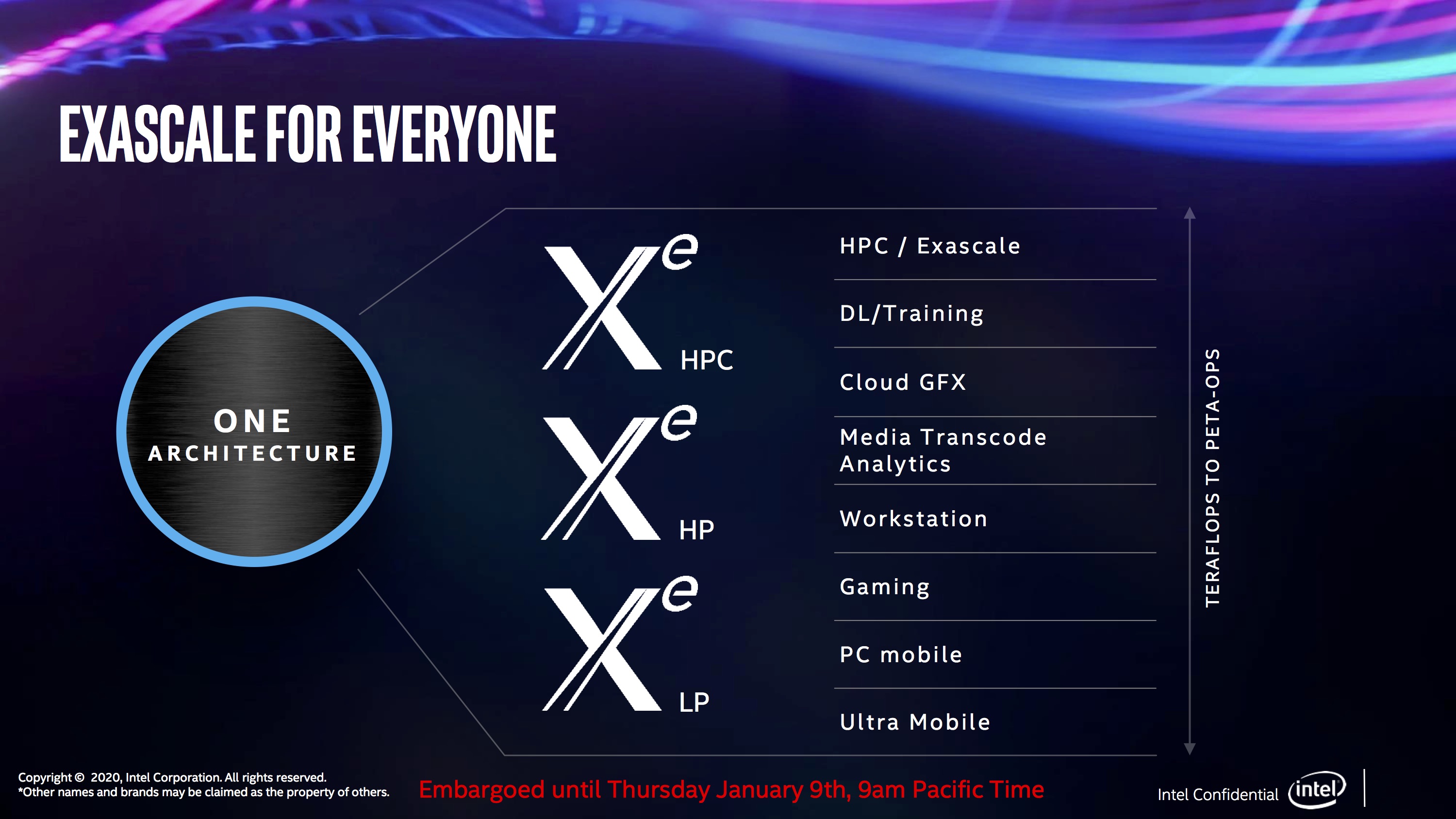
That high end of the market, in turn, is arguably the most important of the three segments for Intel, as well as being the riskiest. The server-class GPUs will be responsible for broadening Intel’s lucrative server business beyond CPUs, along with fending off NVIDIA and other GPU/accelerator rivals, who in the last few years have ridden the deep learning wave to booming profits and market shares that increasingly threaten Intel’s traditional market dominance. The server market is also the riskiest market, due to the high-stakes nature of the hardware: the only thing bigger than the profits are the chips, and thus the costs to enter the market. So under the watchful eye of Raja Koduri, Intel’s GPU guru, the company is gearing up to stage a major assault into the GPU space.
That brings us to the matter of this week’s teaser. One of the benefits of being a (relatively) upstart rival in the GPU business is that Intel doesn’t have any current-generation products that they need to protect; without the risk of Osborning themselves, they’re free to talk about their upcoming products even well before they ship. So, as a bit of a savvy social media ham, Koduri has been posting occasional photos of Intel's Xe GPUs, as Intel brings them up in their labs.
BFP - big ‘fabulous’ package😀 pic.twitter.com/e0mwov1Ch1
— Raja Koduri (@Rajaontheedge) June 25, 2020
Today’s teaser from Koduri shows off a tray with three different Xe chips of different sizes. While detailed information about the Xe family is still limited, Intel has previously commented that the Xe-HPC-based Ponte Vecchio would be taking a chiplet route for the GPU, using multiple chiplets to build larger and more powerful designs. So while Koduri's tweets don't make it clear what specific GPUs we're looking at – if they're all part of the Xe-HP family or a mix of different families – the photo is an interesting hint that Intel may be looking at a wider use of chiplets, as the larger chip sizes roughly correlate to 1x2 and 2x2 configurations of the smallest chip.
And with presumably multiple chiplets under the hood, the resulting chips are quite sizable. With a helpful AA battery in the photo for reference, we can see that the smaller packages are around 50mm wide, while the largest package is easily approaching 85mm on a side. (For refence, an Intel desktop CPU is around 37.5mm x 37.5mm).
Finally, in a separate tweet, Koduri quickly talks about performance: “And..they let me hold peta ops in my palm(almost:)!” Koduri doesn’t go into any detail about the numeric format involved – an important qualifier when talking about compute throughput on GPUs that can process lower-precision formats at higher rates – but we’ll be generous and assume INT8 operations. INT8 has become a fairly popular format for deep learning inference, as the integer format offers great performance for neural nets that don’t need high precision. NVIDIA’s A100 accelerator, for reference, tops out at 0.624 PetaOPs for regular tensor operations, or 1.248 PetaOps for a sparse matrix.
And that is the latest on Xe. With the higher-end discrete parts likely not shipping until later in 2021, this is likely not going to be the last word from Intel and Koduri on their first modern family of discrete GPUs.
Update: A previous version of the article called the large chip Ponte Vecchio, Intel's Xe-HPC flagship. We have since come to understand that the silicon we're seeing is likely not Ponte Vecchio, making it likely to be something Xe-HP based
Source: Intel/Raja Koduri


37 Comments
View All Comments
plopke - Thursday, June 25, 2020 - link
the size of those dies :O.I am very skeptical about the one architecture approach. They putting a lot of categories of workloads all on the same architecture. I am worried it will be ending up with a lot of just good enough in many of them.
Yojimbo - Thursday, June 25, 2020 - link
The one architecture approach is natural. A GPU is like a general purpose parallel processor. The underlying architecture can be applied to different domains efficiently. When they say one architecture they don't mean they won't make changes in individual implementations to differentiate the chips. For example, FP64 vs. no FP64, RT cores vs. no RT cores, cache sizes, which SIPs are included such as encoders and decoders, number and type of memory controllers, etc. With AMD, the CDNA/RDNA is most likely still one architecture, as Intel and NVIDIA would define it. The basic underlying architecture is unified and moves together generation by generation.Duraz0rz - Thursday, June 25, 2020 - link
That's how CPU/GPU design has been for a while now. Every generation uses a single architecture, just scaled differently depending on the application.mode_13h - Thursday, June 25, 2020 - link
Nvidia has differences between their HPC GPUs and consumer models. Intel has differences between their server and consumer cores (things like interconnect and AVX-512, at least). Even AMD has split their HPC GPUs from their consumer architecture (CDNA vs. RDNA).So, I wouldn't say that everyone simply tweaks a knob to instantiate more blocks or less, to address any given market segment. Of course, there are commonalities in just about every case I mentioned besides AMD's GPUs.
sing_electric - Monday, June 29, 2020 - link
Ironically, Nvidia said that Ampere will be both a compute and graphics solution, just as AMD is dividing theirs up.Within an architecture, it's normal to have different chips to hit different size, price and feature points; it's normal to say, offer support for different memory architectures or increase some pipelines while decreasing others.
Plus, even when we're talking about the same silicon there can be real differences: The Radeon VII and Instinct MI50 are the same chip, but with some features turned on/off (no ECC on the VII, for example), and performance severely limited for the double precision FP performance (though they did relent, and went from 1/16 the performance of the MI50 to 1/4 with the flip of a switch).
DanNeely - Thursday, June 25, 2020 - link
Those are the sizes of the chips/IHSes; the actual dies under them are going to be smaller. The package sizes for even the 1x variant are large enough I'm assuming that much of the area under the IHS is taken up by HBM stacks.MikeMurphy - Thursday, June 25, 2020 - link
DanNeely I think you are correct: the HBM stacks would be placed under that heatspreader, which contributes to such a large size.JKflipflop98 - Sunday, June 28, 2020 - link
They're still huge die. They're the biggest you can fab with an EUV litho reticle.Santoval - Sunday, June 28, 2020 - link
EUV has nothing to do with this. Intel will introduce EUV at 7nm. These are still fabbed at 10nm; some of them might even be fabbed at 14nm. Intel's 7nm has not taped out yet so there are no engin. samples (yet).brucethemoose - Thursday, June 25, 2020 - link
The "peta op" tweet almost certainly implies that there's a focus AI performance. And that strategy worked pretty well for Volta/Ampere.