The Intel Lakefield Deep Dive: Everything To Know About the First x86 Hybrid CPU
by Dr. Ian Cutress on July 2, 2020 9:00 AM ESTPerformance Numbers: How To Interpret Them
On the previous page, we covered all three of the initial Lakefield designs. All three are very premium products, either offering a super light and thin clamshell with the Samsung, a foldable display with the Lenovo, or dual 9-inch displays in the case of the Microsoft device. Typically we see these sorts of devices paired with the best-in-class performance hardware, which can cost a lot depending on where it is coming from. Add in the device material cost, and we can easily go north of $999, $1499, or even higher when paired with lots of storage, or items like variable refresh displays. Make no mistake, Lakefield will end up in premium high-cost products.
This means that there will be a certain expectation of performance. Users won’t be satisfied if they get an expensive product with mid-range performance – if they’ve paid top dollar, they want it to exceed in all areas. Performance, battery life, and aesthetics all matter to the end-user when we’re dealing with things like flexible displays or new and exciting form factors on top of everything else.
Now don’t get us wrong here, Lakefield certainly fits many of the criterion of a premium product. It was specifically designed to fit into a small footprint by using novel and complex technology. By using the die-to-die bonding techniques and PoP memory, Intel has put in 174 mm2 of silicon into 12mmx12mm dimensions at only 1mm z-height. It leverages both Intel’s leading edge 10+ manufacturing node as well as Intel’s 22FFL high efficiency manufacturing node, and then optimized layout and manufacturing to ensure it has the most appropriate thermal characteristics for the design. There’s also the ultra-low idle power, supposedly measuring 2-3 mW, which has been an important characteristic in laptops that have been using smartphone processors. Offering substantial idle battery life is a key to marketing this type of product.
However, this page is about performance. Ultimately Lakefield can be compared to a number of products on the market. Numbers in brackets indicate big cores and small cores:
- Intel 7 W Lakefield (1+4) vs Qualcomm Snapdragon 7c (0+8)
- Intel 7 W Lakefield (1+4) vs Intel 6 W Goldmont+ Atom (0+4) N5030
- Intel 7 W Lakefield (1+4) vs Intel 5 W Amber Lake-Y (2+0) m3-8100Y
- Intel 7 W Lakefield (1+4) vs Intel 9 W Ice Lake-Y (2+0) 1005G1
| Comparison Table for Lakefield | |||||
| Intel i7-L16G7 |
AnandTech | Intel i3-1005G1 |
Intel m3-8100Y |
Intel N5030 |
Qualcomm SD 7c |
| Lakefield | SoC | Ice Lake-Y |
Amber Lake-Y |
Goldmont+ | Kryo |
| 1+4 | Core Config | 2+0 | 2+0 | 0+4 | 0+8 |
| 7 W | TDP | 9 W | 5 W | 6 W | ~7 W |
| 1 x SNC 4 x TNT |
CPU | 2 x SNC | 2 x SKL | 4 x GMN+ | 8 x Kryo |
| Gen 11 64 EUs 0.5 GHz |
GPU | Gen 11 32 EUs 0.9 GHz |
Gen 9 24 EUs 0.9 GHz |
Gen 9 18 EUs 750 MHz |
Adreno 618 |
| 4267 | LPDDR | 3733 | LPD3-1866 | 2400 | 4267 |
| Wi-Fi 6* | Wi-Fi | Wi-Fi 5* | - | - | Wi-Fi 6 |
| - | Modem | - | - | - | Cat15/13 |
One processor I missed out here is the Qualcomm Snapdragon 8cx, which is a 4+4 configuration that Qualcomm has specifically built for these sorts of mobile devices. The 4+4 configuration, on paper, might seem unfair to the 1+4 of Lakefield, whereas the 0+8 configuratrion of the Snapdragon 7c is more in line with what we might expect. However, the Snapdragon 7c isn’t actually inside any retail devices right now, having only been on display at Qualcomm’s own event in December.
The thing is, the Snapdragon 7c is set to be in devices competing at the $500 level against entry-level Intel Celeron devices. The 8cx is the premium chip, that ends up in the premium devices. This is where Intel will have difficulty.
On Intel’s own slides, the company performs two main comparisons.
- Benchmarks against Amber Lake-Y, the i7-8500Y in 5W mode
- Benchmarks where the i5-L16G7 runs in 1+4 and 0+4 modes
Benchmarks vs. Intel Amber Lake i7-8500Y
For the first point, Intel promotes the following against Amber Lake:
- +12% single threaded performance, measured by SPEC2006 (3.0 GHz vs 4.2 GHz)
- +70% graphics performance, 3DMark11 comparing HD615 (24 EUs, Gen 9.5 at 1.05 GHz, 2x4 GB LPDDR3-1866) vs HD (64 EUs, Gen11 at 500 MHz, 2x4 GB LPDDR4X-4267)
- +24% power efficiency, score per Watt on WebXPRT 3
- +100% AI workloads on graphics, ResNet50 batch 128 on OpenVINO, comparing
For each of these workloads, there’s something very obvious to pick at.
The first one is SPEC2006, not SPEC2017, and it’s comparing an Amber Lake core to a Sunny Cove core, which as we discussed should have +18% IPC. The frequency difference (assuming both were allowed to turbo to max) is 40% in the favor of Amber Lake, however the Lakefield has a 40% TDP advantage.
On the graphics performance, it’s a substantial mashup – Gen 9 vs Gen 11, 24 EUs vs 64 EUs, 1.05 GHz vs 500 MHz, LPDDR3-1866 vs LPDDR4X-4267. We know that Intel is going wide and slow with Lakefield, and the fact that Lakefield has an additional 40% TDP to help the graphics and CPU cores, I suspect that each chip was battling to find the right balance of power to the CPU or power to the GPU.
On the AI workload, this benchmark has been hand-picked. Intel has done an offline Resnet-50, and run the CPUs in batches. With the GPU being wide and slow, there is the question as to whether the GPU would be competitive in batch-1 type scenarios. Again, there’s also a TDP difference here, as well as a memory difference that explains the raw performance change.
Benchmarks Against Lakefield in 1+4 Mode against 0+4 Mode
For the second set of benchmarks, Intel promotes +33% higher web performance and 17% better power efficiency by adding a big core to a quartet of small cores – essentially comparing a full fat Lakefield against a quad-core Atom design.
What this means is that Lakefield, by and large, will perform the same as a quad-core Atom in almost all tasks, especially heavy tasks. Given that we haven’t had a new Atom platform since 2017, and it’s been even longer since we saw Atom notebooks in a big way, I can guarantee that a lot of users will look at Lakefield and compare it to big-core designs. Intel has also tripped over its own feet in not comparing the performance to any of Qualcomm’s designs. The cost would seem to put it square against the Snapdragon 8cx, however the core layout suggests the 7c would be a fairer fight. Putting Intel’s AI test against Qualcomm’s hardware would also make for an interesting comparison.
Another thing to note, which Intel glossed over, that most people are going to be really concerned about.
What The Big Core Is Actually For
I’ve mentioned a few times in this piece that the big Sunny Cove core is more for end-user latency driven interactions, such as tapping on the screen, typing on the keyboard. When it comes to loading a web page, this blurs the line between response and workload, depending on the browser and how it manages threads.
Now, if we take a traditional high load single threaded workload, such as say, rendering. Which core will it run on? A lot of Intel’s marketing materials, as well as considering the layout of the chip, might get a reasonable end-user to expect that it would run on the high-performance single core. However, consider two things: firstly, rendering a frame is not a latency-driven interaction. Secondly, how many processes are running in the background? Both of these elements would point to the operating system pushing the workload, despite being single threaded, onto the Tremont Atom cores.
At the time of writing, Notebookcheck is the only outlet to publish data from an early look on Samsung’s Galaxy Book S. If we take a single threaded rendering workload, like Cinebench R15, then Lakefield scores 88 points, while the Amber Lake that Intel used in its slides scores 129, a +46% performance uplift to the older Amber Lake system. What in the world is going on? It’s running on the Atom cores.
Our recommendation, for anyone wanting to test the performance of that single Sunny Cove core, is to implement an affinity mask on the software being used. If the software only knows that one core exists, then it can only run on that core. This is how we suspect that Intel achieved the single core performance gains in benchmarks like SPEC2006. However Intel has more tools at its disposal – there’s a chance that the scheduler for these systems might ignore affinity masks in order to maintain a thermal balance in the design. We must wait until we get a sample in for ourselves.
To a certain extent we see this in the Cinebench R15 multi-threaded test. With a standard 5 thread processor, if you run a standard nT test, we expect it to fill all the cores to give the best performance. In Notebookcheck’s article, we can see that the scheduler has evicted the workload from the big core. This is likely due to power/thermal hotspot reasons.
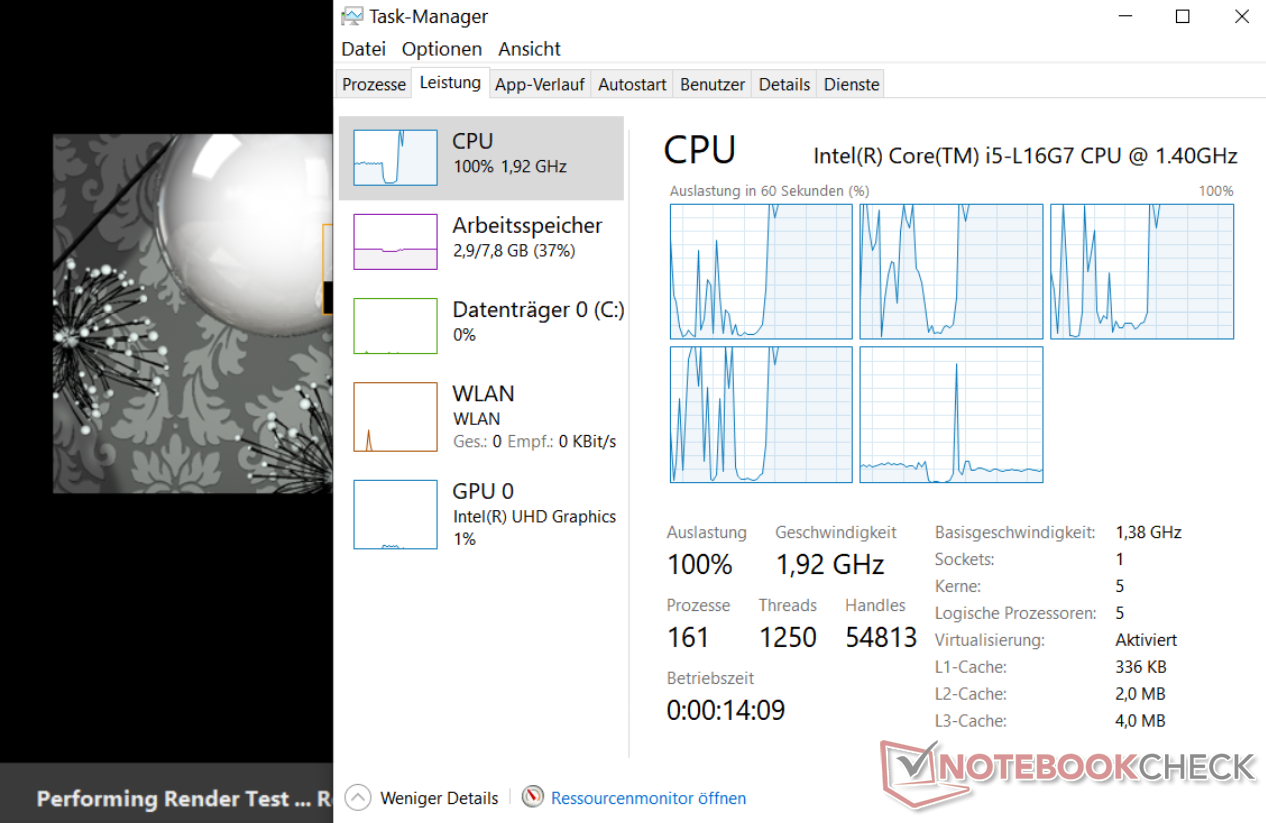
Source: Notebookcheck
In the task manager on the right, we see the first four Atom cores running at 100% while in the multi-threaded test, while the large Sunny Cove core is relatively idle. Note that the CPU is running at 1.9 GHz, and not the 2.8 GHz that Intel has promoted is the all-core turbo for this product.
But the bottom line is that in most cases, expect Lakefield to perform similar to four Atom cores, just above Goldmont Plus, and not like any of the Skylake/Ice Lake Core products and its derivatives.


221 Comments
View All Comments
returnzer0 - Friday, July 3, 2020 - link
So no, they did not, in fact, read the same article.s.yu - Monday, July 6, 2020 - link
Mystery solved!vanilla_gorilla - Friday, July 3, 2020 - link
https://www.anandtech.com/show/15877/intel-hybrid-..."At the top is the single Sunny Cove core, also present in Ice Lake. Intel has stated that it has physically removed the AVX-512 part of the silicon, however we can still see it in the die shot. This is despite the fact that it can’t be used in this design due to one of the main limitations of a hybrid CPU. We’ll cover that more in a later topic."
It was NOT physically removed but it cannot be used so it doesn't really matter. In practice this will have no AVX-512.
dotjaz - Friday, July 3, 2020 - link
Also "However, all modern software assumes a homogeneous processor", that's why they have to support exactly the same ISA extensions. I didn't realise Windows is the only modern software in existence.Meteor2 - Friday, July 3, 2020 - link
Why so rude, dotjaz?dotjaz - Saturday, July 4, 2020 - link
So which part is rude? Is this rude asking you what's rude? Sorry your feelings got hurt. There, happy now?jospoortvliet - Sunday, July 5, 2020 - link
Linux also expects it. Modern enough?jeremyshaw - Thursday, July 2, 2020 - link
Good. This action ensures this segment of products will be easier to emulate on arm, helping to tear these products away from Intel's grasp.Kangal - Sunday, July 5, 2020 - link
To be honest, this is a great innovation.It's just the execution is quite lacking, and on top of that, it's a couple years too late.
Just imagine a SoC such as:
3x Big processor (Intel Core M), eg/ Core i7-8500Y
5x Small processor (Intel Atom), eg/ Atom x7-Z8750
Dynamic Scaling:
(Idle) 4x Small Cores run at 500MHz at Idle
(Very-low power) 4x Small Cores clock starting at 1.0GHz
(Low-power use) 5x Small Cores clock upto 2.5GHz
(Medium power) 3x Big Cores starting at 1.5GHz, 5x Small Cores upto 2.5GHz
(Regular power) 3x Big Cores at 2.0GHz, 5x Small Cores at 2.0GHz
(High-power use) 3x Big Cores at 3.0GHz, 5x Small Cores at 2.0GHz
(Very-high power) 3x Big Cores at 4.0GHz, 5x Small Cores at 2.5GHz
(Max-power use) 1x Big Cores at 5.0GHz, 2x Big Cores at 4.0GHz, 5x Small Cores at 2.5GHz
Kangal - Sunday, July 5, 2020 - link
Now imagine all of this, competing against AMD.Their 12nm node is fairly competitive against Intel's 14nm. And their Zen+ architecture is somewhat competitive against Intel's Skylake architecture. So comparing the above Hybrid Processor, to a 4c/8t (eg/ Ryzen-3780U). Well that's a no contest victory for Intel. And AMD would struggle to fit those technologies into a 8-core laptop processor, so there would be no threat from above.
Once AMD steps up to either Zen2 architecture, or 7nm node, or both!...
....that's when things get heated. Since in the 15W / Ultrabook market, the above setup by Intel would secure a slim victory against similar 4c/8t AMD processor. But when you step up to the 25W / Laptop market, then AMD will pull ahead with their 8c/16t processor. However at least in this scenario, Intel has a good showing of their competitiveness and capabilities. That works upto 2021, but after that, Intel will have to make noticeable performance improvements to both Big/Small Core architectures, AND, they will have to make substantial efficiency improvements on the lithography side (maybe execute on their 8nm nodes, versus TSMC's 5nm).
First question, why use examples of Cherry Trail and Amber Lake?
Well, they're both on Intel's (pretty good) 14nm node. Also this is the most efficient "Small Core" Atom architecture that Intel has. Later produced Intel Pentium/Celeron/Atom processors come from the same family, however, they're designed for higher energy consumption. Whereas the "Big Core" stated above is a Core M processor (now rebranded as a Core i7-Y), and it is the latest and best they have when it comes to performance whilst maintaining efficiency.
Why the 3/5 Split you may ask?
Well, the most useful is the first/main thread. Followed closely by the second thread as most code has evolved for Dual-Cores in the past 20 years. And somewhat important is the third core, as we've also had an evolution to Quad-Cores in the past 10 years. However, most code hasn't made the full transition from single to dual threads, the same way that dual threads haven't translated well to quad threads. So instead of 2+6 split, which will have some performance drops on Quad thread code, it's better to go for 3+5. So you may ask, then why not just go for an even 4+4 split? Well, most of those quad threads don't utilise the 4th core very well, so we can make do by relegating that to a Small Core instead. This saves us some efficiency, which is what we want to achieve with this concept in the first place. The least energy using split would be 0+8. The most performant split would be 8+0. So this 3+5 split is basically the best of both worlds, since you will get 90% of the single-threaded performance, 70% of the multi-threaded performance, and 50% of the energy expenditure characteristics. So it's not perfect, but it's the closest you can get there... until the code evolves further. And we've started transitioning codes running for 8-core processors only around 2015-2017, so there's a good chance we aren't going to see the evolution tipping point until around 2025.