Russia’s Elbrus 8CB Microarchitecture: 8-core VLIW on TSMC 28nm
by Dr. Ian Cutress on June 1, 2020 8:00 AM EST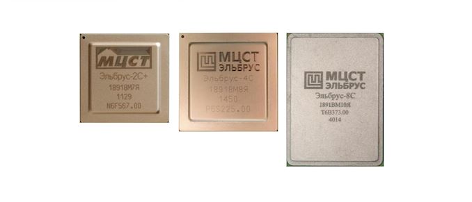
All of the world’s major superpowers have a vested interest in building their own custom silicon processors. The vital ingredient to this allows the superpower to wean itself off of US-based processors, guarantee there are no supplemental backdoors, and if needed add their own. As we have seen with China, custom chip designs, x86-based joint ventures, or Arm derivatives seem to be the order of the day. So in comes Russia, with its custom Elbrus VLIW design that seems to have its roots in SPARC.
Russia has been creating processors called Elbrus for a number of years now. For those of us outside Russia, it has mostly been a big question mark as to what is actually under the hood – these chips are built for custom servers and office PCs, often at the direction of the Russian government and its requirements. We have had glimpses of the design, thanks to documents from Russian supercomputing events, however these are a few years old now. If you are not in Russia, you are unlikely to ever get your hands on one at any rate. However, it recently came to our attention of a new programming guide listed online for the latest Elbrus-8CB processor designs.
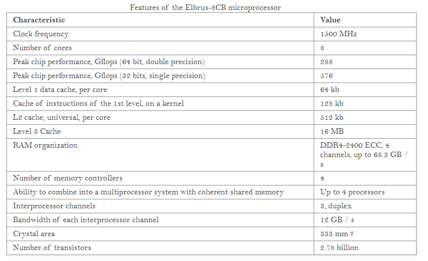
The latest Elbrus-8CB chip, as detailed in the new online programming guide published this week, built on TSMC’s 28nm, is a 333 mm2 design featuring 8 cores at 1.5 GHz. Peak throughput according to the documents states 576 GFLOPs of single precision, with the chip offering four channels of DDR4-2400, good for 68.3 GB/s. The L1 and L2 caches are private, with a 64 kB L1-D cache, a 128 kB L1-I cache, and a 512 kB L2 cache. The L3 cache is shared between the cores, at 2 MB/core for a total of 16 MB. The processor also supports 4-way server multiprocessor combinations, although it does not say on what protocol or what bandwidth.
It is a compiler focused design, much like some other complex chips, in that most of the optimizations happen at the compiler level. Based on compiler first designs in the past, that typically does not make for a successful product. Documents from 2015 state that a continuing goal of the Elbrus design is x86 and x86-64 binary translation with only a 20% overhead, allowing full support for x86 code as well as x86 operating systems, including Windows 7 (this may have been updated since 2015).
The core has six execution ports, with many ports being multi-capable. For example, four of the ports can be load ports, and two of the ports can be store ports, but all of them can do integer operations and most can do floating point operations. Four of the ports can do comparison operations, and those four ports can also do vector compute.
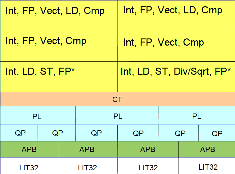
Elbrus 8CB Core
This short news post is not meant to be a complete breakdown of the Elbrus capabilities – we have amusingly joked internally at what frequency a Cortex X1 with x86 translation would match the capabilities of the 8-core Elbrus, however users who want to get to grips with the design can open and read the documentation at the following address:
http://ftp.altlinux.org/pub/people/mike/elbrus/docs/elbrus_prog/html/index.html
The bigger question is going to be how likely any of these state-funded processor development projects are going to succeed at scale. State-funded groups should, theoretically, be the best funded, however even with all the money in the world, engineers are still required to get things done. Even if there ends up being a new super-CPU for a given superpower, there will always be vested interests in an amount of security though obscurity, especially if the hardware is designed specifically to cater to state-secret levels of compute. There's also the added complication of the US government tightening its screws around TSMC and ASML to not accept orders from specific companies - any plans to expand those boundaries could occur, depending how good the products are or how threatened some nations involved feel.
Source: Blu (Twitter)


93 Comments
View All Comments
mshigorin - Monday, June 1, 2020 - link
Well I'm only a rocket amateur (nitrofilm and gunpowder, ya'know) but Buran got landed automatically under Elbrus guidance, from what I've heard...nasdaq13 - Sunday, June 7, 2020 - link
We also had a PS-2000. https://computer-museum.ru/histussr/11-1.htmmshigorin - Monday, June 1, 2020 - link
The only "real world" problem -- or should I say woe? -- is lots of javascrapt and JS JIT being underoptimized on e2k so far (the guys tell that there's still a lot to do there). Said that, I use Elbrus 801-PC for my daily work at Basealt Ltd, and no one forced me to switch from my then-recent i5 based notebook two years ago.Wilco1 - Monday, June 1, 2020 - link
For comparison, peak double FLOPS per CPU:Elbrus @ 1.5GHz: 36
Cortex-X1 @ 3GHz: 48
A64FX @ 2.2GHz: 70.4
DanNeely - Monday, June 1, 2020 - link
With Elbrus built on an ancient 28nm process that comparison doesn't look bad. OTOH as a desktop part it's core is probably a lot bigger than ARMs mobile cores are; and it ignores that VLIW for general purpose compute has never really worked in the real world. It can be useful in more constrained scenarios, eg AMD VLIW5 was a good fit for DX9s 5 step setup; but fitting enough ops to fill up the VLIW was hard enough with DX10's more flexible design that later models dropped down to VLIW4; before they dropped it entirely with GCN.mshigorin - Monday, June 1, 2020 - link
I know a Russian hacker who contested AMD developers with optimizing that code and did it in under three months -- the job they couldn't complete in a year... the commits are out there in radeonsi driver.And as I've said above, the only real world application where I really with things would run apx. 1.5X faster on 801-PC is javascrapt in fx52 they've ported for e2k so far (with fx68 and some chromium reportedly underway either) -- still e.g. maps.yandex.ru work good for me already, and it's one of the most js-intensive oft-used webapps for me.
mshigorin - Monday, June 1, 2020 - link
*where I really wish, of course :-)AlB80 - Monday, June 1, 2020 - link
Elbrus 5 gen can issue 6 fma vector instructions (vector width = 2 doubles / 4 floats).ARM Cortex-X1 can issue 4 fma vector instructions (4 / 8).
Fujitsu A64FX can issue 2 fma vector instructions (16 / 32).
Jorgp2 - Monday, June 1, 2020 - link
How does it compare to Itanium?mshigorin - Monday, June 1, 2020 - link
It's alive.