Arm Announces The Mali-G78 GPU: Evolution to 24 Cores
by Andrei Frumusanu on May 26, 2020 9:00 AM ESTMore Scaling, Different Frequency Domains
For people unfamiliar with the Mali-G77 and the Valhall GPU architecture, I highly recommend on catching up on last year’s deep dive into the changes of the design, as very much the majority of those key elements are still very much present on the new Mali-G78.
Read: Arm's New Mali-G77 & Valhall GPU Architecture: A Major Leap

From a high top-level perspective, the biggest visible change for the new G78 is the promise that it’ll be able to scale up again to 24 GPU cores. For the last few generations of Mali architectures Arm seemingly has been playing catch-up with trying to consolidate their GPU cores into bigger building blocks, with each successive GPU release always trying to improve the per-core performance rather than just adding in more cores.
Last year when Arm had released the G77 the company did exactly this, as pretty much a G77 core is roughly equal in capability to two G76 cores. Chipsets such as the Exynos 990 and Dimensity 1000 had “reasonable” core numbers of 11 and 9, bringing down the core count compared to past Mali GPUs. There’s still a stark contrast to other mobile GPU microarchitectures, such as Qualcomm’s current 2-core Adreno or Apple’s 4-core designs. The problem with scaling up performance with smaller cores is that this is never as power efficient as scaling up fewer bigger cores, as the latter have less duplication of functions, meaning fewer overhead transistors to burn power.
In a sense, the Mali-G78 here scaling up to 24 cores again seems like a step backwards. I had feared that the company had still gone with too small a core on the G77/Valhall architecture, as now seemingly we’re going to have core-count creep again in order to scale up performance.
Configuration wise, the one thing that Arm did away with is the option of a 4MB L2. While the company says it still retains this capability, no vendor had ever chosen to go with such an implementation, with essentially all Mali GPUs to date using 2MB options.

From an execution core perspective, the Mali-G78 remains identical to last year’s G77. The big changes to past G76 designs and prior was the consolidation of multiple execution engines into a single much wider unit, that had also doubled up on the SIMD and warp width of the execution lanes.
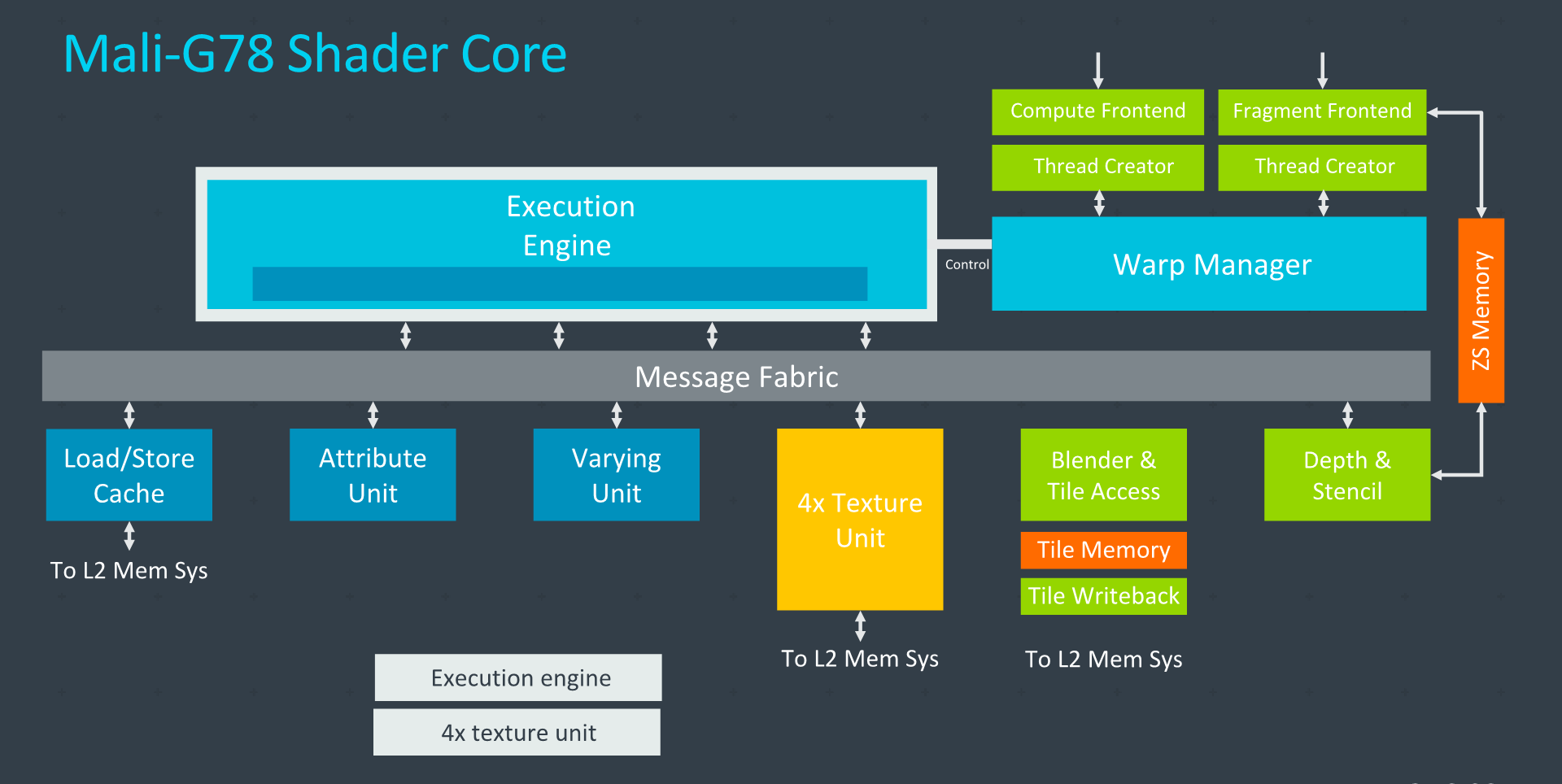
The overall core block diagram also remains the same. Key aspects here is the single execution engine, and a quad-pumped texture unit that supports up to 4 texels per clock filtering capability and 2 pixel per clock render output.
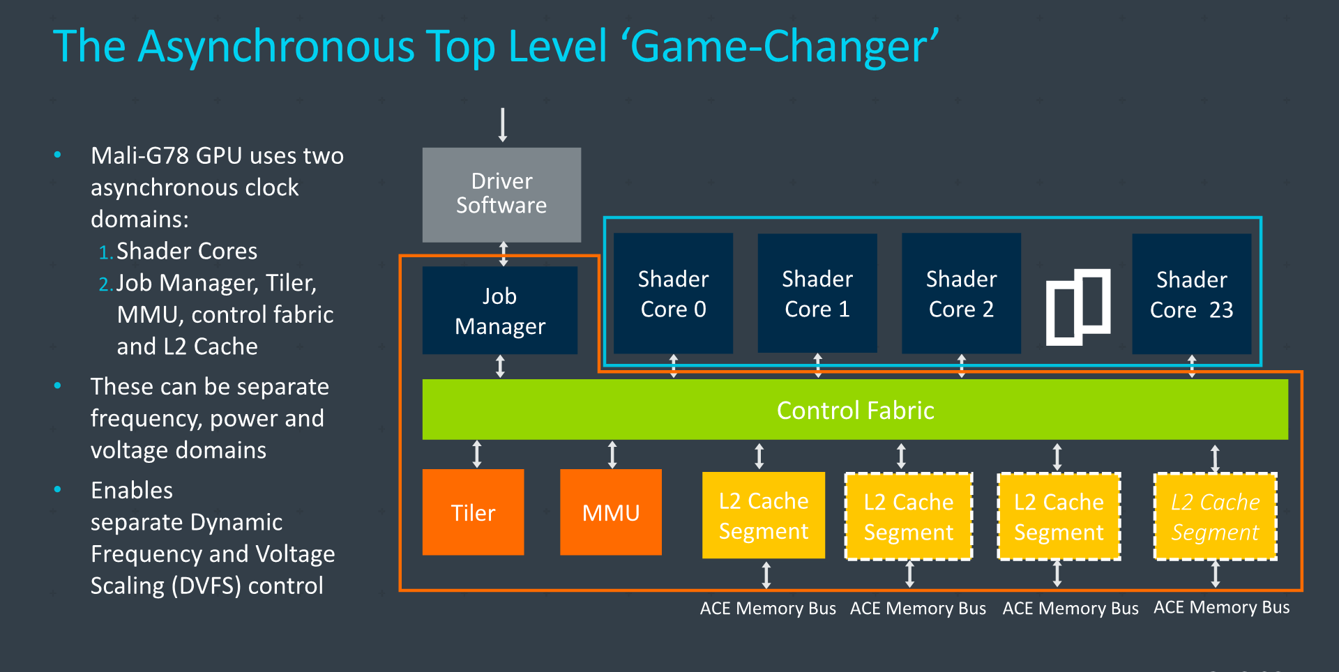
The one key changed of the Mali-G78 that Arm had talked about the most, was the change from a single global frequency domain for the whole GPU to a new two-tier hierarchy, with decoupled frequency domains between the top-level shared GPU blocks, and the actual shader cores.
In essence, Arm is introducing asynchronous clock domains within the GPU, allowing the shader cores to operate at a different frequency to the rest of the GPU. This actually can go both ways, with either the cores going faster, or actually slower, than the memory subsystem and tiler blocks.
The main rationale behind this change is to address two problems: geometry throughput and memory throughput for different workloads. In essence, Arm’s GPU architecture has one big problem, and that is that for the GPU to push out a higher number of polygons on screen, the architecture has no option other than trying to scale up its operating frequency. The tiler and geometry engine here are still only able to process a single triangle per clock, and that metric is fixed and non-scalable across GPU configurations.
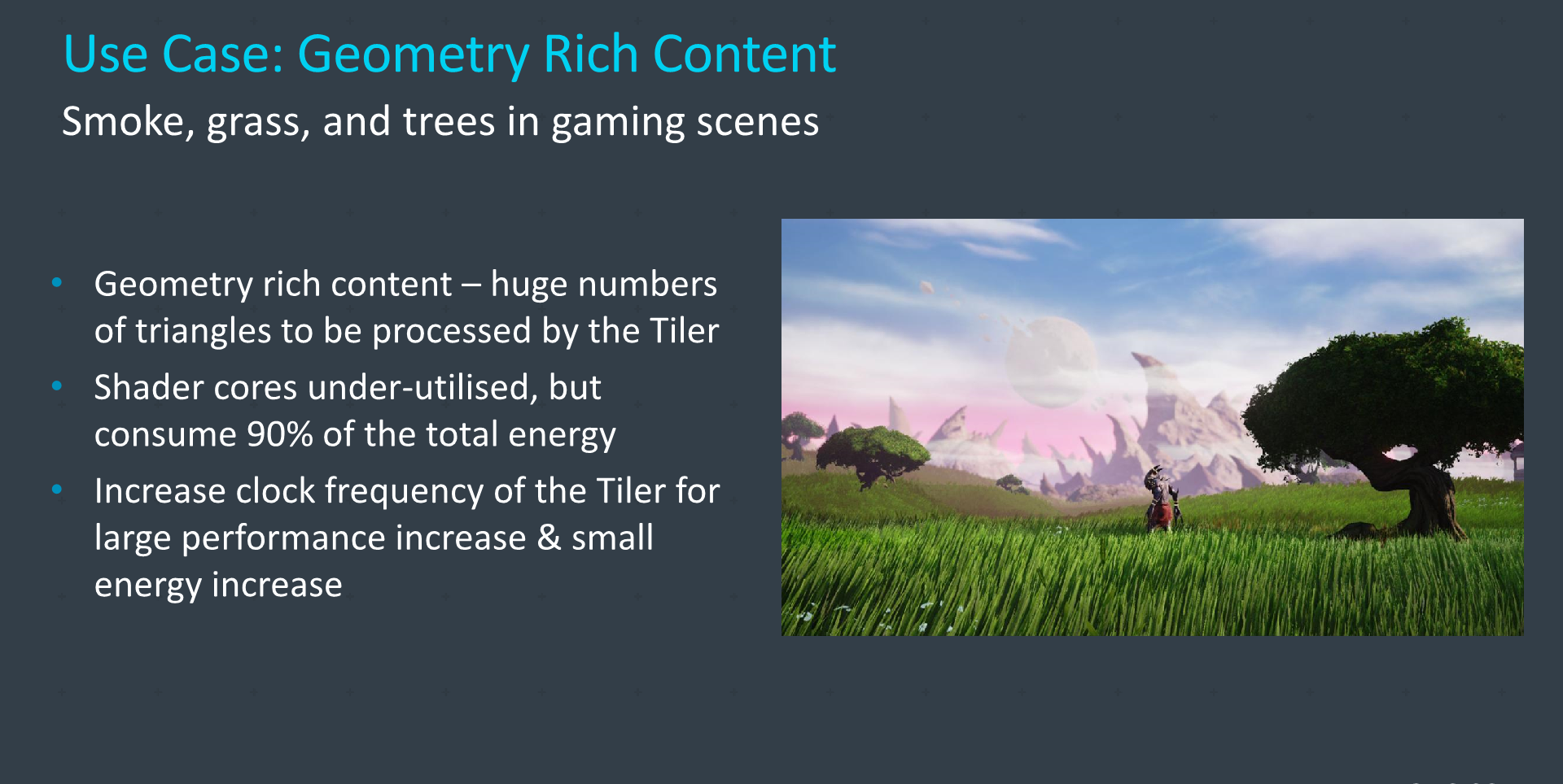
In recent years, we’ve seen a change in the mobile GPU landscape, particularly with desktop originating titles such as Fortnite and PUBG making it to our smartphones. One aspect of these newer games is that they’re much more geometry heavy than your usual past mobile titles, and seemingly this has become a problem for the Mali architecture.
Arm’s introduction of different frequency domains is a relatively smart solution to the problem. If you can decouple the frequency between your tiler and geometry engine and the actual GPU cores, you can actually solve the issue of there being an imbalance between geometry throughput that’s not scalable in width, and the core-scalable throughput of compute, texturing and pixel engines.
Furthermore, this decoupling also allows to operate the GPU to operate at different voltages between the two domains. The slower domain would be able to operate at a lower frequency and voltage, thus gaining power efficiency, all whilst in theory not impacting performance. The problem with this is that it now forces the SoC vendor to implement an additional voltage domain and power rail – which can add to the costs of the system.
While this all sounds good, I can’t help but think of this being a band-aid solution to a more fundamental problem of the Valhall GPU architecture. The fact that the architecture is only able to support one tiler and geometry engine is the core limitation that lead to this asynchronous top level to be implemented. In the desktop world, we saw the difficult switch to multi-geometry engine architectures almost a decade ago, and it seems to be that the need of such a redesign is also creeping up to the mobile space.
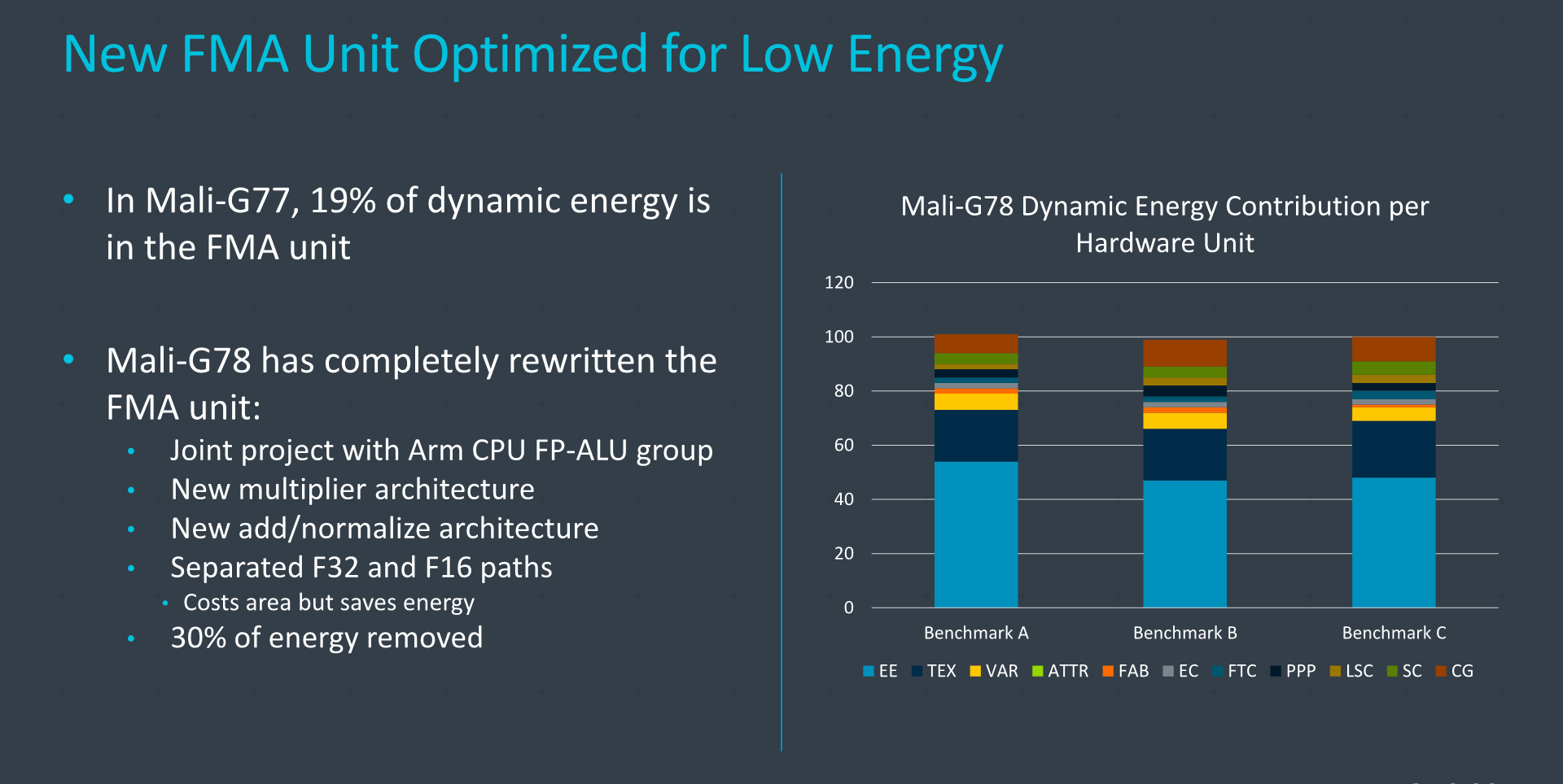
Another significant change the G78 bring is the complete rewrite of its FMA engines. This is said to be a joint-effort with the Arm CPU group, and has resulted in a 30% energy reduction. Key aspects here were the physical separation of the FP32 and FP16 paths, which does cost more transistors and area to implement, but it will have less actual switching transistors when actively operating.
In the G77, Arm says that the FMA units alone accounted for 19% of the dynamic switching energy of the whole GPU. A 30% reduction of that slice means an overall 5-6% improvement of the energy efficiency of the whole GPU, just by that one change.

Finally, a change in the efficiency of the design is improvements in the tiler that allows it to better scale with the increased core counts. The core’s cache shave also had they cache maintenance algorithms improved with better dependency tracking, allowing for the cores to more smartly handle cache data and to avoid unnecessary moving of data which results in a reduction in internal GPU bandwidth as well as power (Or more performance thanks to more available bandwidth).


36 Comments
View All Comments
tkSteveFOX - Wednesday, May 27, 2020 - link
Apart from MTK and Huawei most will drop using Mali Cores as the architecture doesn't scale well at all.Anything over 7-8 cores and you start to lose performance and get the consumption up.
When Samsung finally unveil their RDNA powered GPU, even Apple's cores might lose their crown.
I doubt it will be very power efficient though, just like Apple's.
lightningz71 - Wednesday, May 27, 2020 - link
Haven't the various mobile RISC cores gotten very close to hitting the wall with respect to memory bandwidth? Feeding the G78 in a full-house config with enough data to allow it to reach it's full throughput potential would require fairly massive amounts of RAM bandwidth. All that bandwidth will require some very wide channels and a lot of memory ICs on the phone motherboards, or, it'll require some quite power hungry HBM stacks. At best, we get a couple of channels of low power DRAM that spends as much time as possible in low power mode. I just don't see it being very useful on a mobile device. At the very best, if it's used in an ARM Windows laptop, and if it gets a solid memory subsystem attached to it, it MAY be competitive with other iGPU solutions available in the market. However, once you go down that road, you have to ask yourself, is it worth putting that many resources into the CPU and its memory subsystem when there are available low power dGPU solutions out there that will still run rings around it in performance and not cost any more per unit to integrate into your solution? Even if it costs a bit more power to do so, in a laptop, you have a much larger form factor and much larger power budgets to play with.ballsystemlord - Thursday, May 28, 2020 - link
Spelling error:"The core's cache shave also had they cache maintenance algorithms improved with better dependency tracking,..."
"the" not "they":
"The core's cache shave also had the cache maintenance algorithms improved with better dependency tracking,..."
Lobstermobster - Saturday, June 6, 2020 - link
How can we compare this new mobile GPU to others made by Qualcomm, Nvidia and Imagination? How many teraflops do these mobile GPUs have? I know the Switch uses a Tegra chip that can go up to 1 teraflops in dock modeiphonebestgamephone - Sunday, June 7, 2020 - link
Whats the use of knowing the flops anyway.IUU - Friday, October 2, 2020 - link
"Whats the use of knowing the flops anyway." I believe it is one of the most important metrics to know. Because a chip will always perform a certain percentage of its theoretical performance, often about 60 to 70% of theoretical. So , if a chip's theoretical performance is say X5 compared to another chip, no-one can fool you with the usual nonsense, "yes but it is real world performance that matters" . Because a x5 theoretical performance wins hands down in real world scenarios, no matter what marketing gimicks would want you to believe.That said , just consider , the modern fashion of hiding details about architecture , of a lot of companies, lately even by Intel, and you will see , there is an effort to go by marketing only to hide potential weaknesses.