AMD’s New EPYC 7F52 Reviewed: The F is for ᴴᴵᴳᴴ Frequency
by Dr. Ian Cutress on April 14, 2020 9:45 AM EST- Posted in
- CPUs
- AMD
- Enterprise
- Enterprise CPUs
- EPYC
- SP3r2
- CPU Frequency
- Rome
- 7Fx2
Frequency Ramp, Latency and Power
Frequency Ramp
One of the key items of a modern processor is its ability to go from an idle state up to a peak turbo state. For consumer workloads this is important for the responsiveness of a system, such as opening a program or interacting with a web page, but for the enterprise market it ends up being more relevant when each core can control its turbo, and we get situations with either multi-user instances or database accesses. For these systems, obviously saving power helps with the total cost of ownership, but being able to offer a low latency transaction in that system is often a key selling point.
For our 7F52 system, we measured a jump up to peak frequency within 16.2 milliseconds, which links in really well with the other AMD systems we have tested recently.
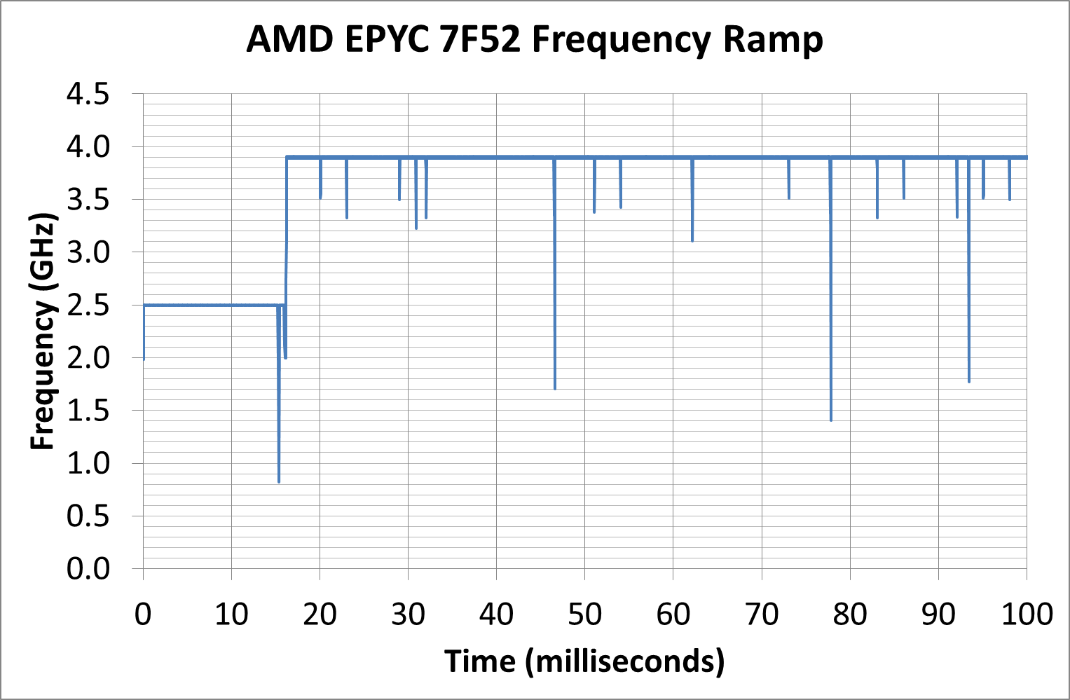
In a consumer system, normally we would point out that 16 milliseconds is the equivalent to a single frame on a 60 Hz display, although for enterprise it means that any transaction normally done within 16 milliseconds on the system is a very light workload that might not even kick up the turbo at all.
Cache Latency
As we’ve discussed in the past, the key element about Cache Latency on the AMD EPYC systems is the L3 cache – the way these cores are designed, with the quad-core core complexes, means that the only L3 each core can access is that within its own CCX. That means for every EPYC CPU, whether there is four cores per CCX enabled, or if there is only one core per CCX enabled, it only has access to 16 MB of L3. The fact that there is 256 MB across the whole chip is just a function of repeating units. As a result, we can get a cache latency graph of the following:

This structure mirrors up with what we’ve seen in AMD CPUs in the past. What we get here for the 7F52 is:
- 1.0 nanoseconds for L1 (4 clks) up to 32 KB
- 3.3 nanoseconds for L2 (13 clks) up to 256 KB,
- 4.8-5.6 nanoseconds (19-21 clks) at 256-512 KB (Accesses starting to miss the L1 TLB here)
- 12-14 nanoseconds (48-51 clks) from 1 MB to 8 MB inside the first half the CCX L3
- Up to 37 nanoseconds (60-143 clks) at 8-16 MB for the rest of the L3
- ~150 nanoseconds (580-600+ clks) from 16 MB+ moving into DRAM
Compared to one of our more recent tests, Ryzen Mobile, we see the bigger L3 cache structure but also going beyond the L3 into DRAM, due to the hop to the IO die and then out to the main memory there’s a sizeable increase in latency in accessing main memory. It means that for those 600 or so cycles, the core needs to be active doing other things. As the L3 only takes L2 cache line rejects, this means there has to be a lot of reuse of L3 data, or cyclical math on the same data, to take advantage of this.
Core-to-Core Latency
By only having one core per CCX, the 7F52 takes away one segment of its latency structure.
- Thread to Thread in same core: 8 nanoseconds
- Core to Core in same CCX: doesn't apply
- Core to Core in different CCX on same CPU in same quadrant: ~110 nanoseconds
- Core to Core in different CCX on same CPU in different socket quadrant: 130-140 nanoseconds
- Core to Core in a different socket: 250-270 nanosecons
All of the Power
Enterprise systems, unlike consumer systems, often have to adhere to a strict thermal envelope for the server and chassis designs that they go into. This means that, even in a world where there’s a lot of performance to be gained from having a fast turbo, the sustained power draw of these processors is mirrored in the TDP specifications of that processor. The chip may offer sustained boosts higher than this, which different server OEMs can design for and adjust the BIOS to implement, however the typical expected performance when ‘buying a server off the shelf’ is that if the chip has a specific TDP value, that will be the sustained turbo power draw. At that power, the system will try and implement the highest frequency it can, and depending on the microarchitecture of the power delivery, it might be able to move specific cores up and down in frequency if the workload is lighter on other cores.
By contrast, consumer grade CPUs will often boost well beyond the TDP label, to the second power limit as set in the BIOS. This limit is different depending on the motherboard, as manufacturers will design their motherboards beyond Intel specifications in order to supplement this.
For our power numbers, we take the CPU-only power draw at both idle and when running a heavy AVX2 load.
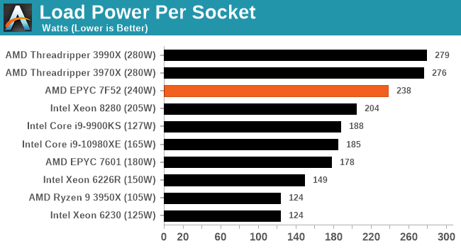
When we pile on the calories, all of our enterprise systems essentially go to TDPmax mode, with every system being just under the total TDP. The consumer processors give it a bit more oomph by contrast, being anywhere from 5-50% higher.
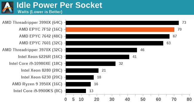
In our high performance power plan, the AMD CPUs idle quite high compared to the Intel CPUs – both of our EPYC setups are at nearly 70 W per processor a piece, while the 32C Threadripper is in about that 45 W region. Intel seems to aggressively idle here.


97 Comments
View All Comments
beginning - Tuesday, April 14, 2020 - link
Thank you for this review! Quite useful. I would like to see performance comparisons on multi-threaded workloads too.anonomouse - Tuesday, April 14, 2020 - link
Looking at memory latency chart, it doesn't look like the second half of the LLC is actually any farther - that's just the limit of the range that the L2 TLB (2K entries @4K pages) can cover. The additional latency beyond 8MB is probably because requests are now causing table walks, and that is also clear from Andrei's corresponding chart for the client version in 3700x/3900x. Were these results cross-checked with each other before publication?One way to verify this would be to enable huge pages and see if the memory latency profile you're claiming looks different.
boozed - Tuesday, April 14, 2020 - link
"AMD is hoping to stag that first second rung of the ladder"What does this expression mean?
UnknownKnolwdge - Tuesday, April 14, 2020 - link
Look up ladder logic on wikipedia, search for rung.It's associated with relay logic and old style PLC programming.
boozed - Tuesday, April 14, 2020 - link
Thanks but I'm not convinced that's itSmell This - Wednesday, April 15, 2020 - link
"AMD is hoping to stag that first second rung of the ladder."________________________________________________
Two things:
1) I suspect the meaning is 'the next step up;' and
2) 'snag' instead of 'stag'
:-)
madwolfchin - Tuesday, April 14, 2020 - link
This processor should be targeted for Single threaded workload, why are all the benchmark multi threaded. Would also like to see the IPC performance since there is a large increase of cachenicamarvin - Wednesday, April 15, 2020 - link
Mr. Cutress on this article you have the 3950X and 3990X as "Rome" uArch, but in Fact they are Matisse for 3950X and Castle Peak for the 3990XMachinus - Wednesday, April 15, 2020 - link
I wish there was more than one CPU maker in the market right now. These chips looks great, but there is no competition.Threska - Wednesday, April 15, 2020 - link
Not specifically in this niche, but ARM (and equivalent) haven't gone anywhere.