AMD’s Mobile Revival: Redefining the Notebook Business with the Ryzen 9 4900HS (A Review)
by Dr. Ian Cutress on April 9, 2020 9:00 AM ESTRenoir: Latency, Caching, and Turbo
Chiplets vs Monolithic
To date, AMD has launched Desktop Ryzen 3000, Threadripper 3000, and EPYC 7002 (Rome) with Zen 2 cores. For all these products, it has placed its Zen 2 cores inside chiplets that connect to a central IO die, which then talks to other chiplets or the main system. In Ryzen 3000 Desktop, we have one or two chiplets paired with an IO die that can handle 24 PCIe 4.0 lanes and two memory channels. In Threadripper 3000, we have up to eight chiplets with an IO die that can handle 64 PCIe 4.0 lanes and four memory channels. In EPYC 7002 (Rome), we have up to eight chiplets with an IO die that can handle 128 PCIe 4.0 lanes and eight memory channels.
For Ryzen Mobile 4000, there are no chiplets – instead we have a traditional single die, which is referred to as a monolithic design. Both the chiplet design and monolithic designs have various benefits and weaknesses.
For the chiplet design, going that route for expensive processors actually helps with costs, yields, and frequency binning. This has also enabled AMD to launch these products earlier, with the end result being better per-core performance (through binning), taking advantage of different process nodes, and providing an overall chip with more die area than a single chip can provide.
The downside of this chiplet design is often internal connectivity. In a chiplet design you have to go ‘off-chip’ to get to anywhere else, which incurs a power and a latency deficit. Part of what AMD did for the chiplet designs is to minimize that, with AMD’s Infinity Fabric connecting all the parts together, with the goal of the IF to offer a low energy per bit transfer and still be quite fast. In order to get this to work on these processors, AMD had to rigidly link the internal fabric frequency to the memory frequency.
With a monolithic design, AMD doesn’t need to apply such rigid standards to maintain performance. In Ryzen Mobile 4000, the Infinity Fabric remains on the silicon, and can slow down / ramp up as needed, boosting performance, decreasing latency, or saving power. The other side is that the silicon itself is bigger, which might be worse for frequency binning or yield, and so AMD took extra steps to help keep the die size small. AMD was keen to point out in its Tech Day for Ryzen Mobile that it did a lot of work in Physical Design, as well as collaborating with TSMC who actually manufactures the designs, in order to find a good balance between die size, frequency, and efficiency.
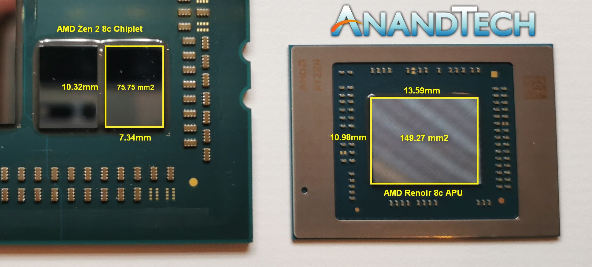
The Renoir silicon is ~150 square millimeters. (AMD’s official number is 156 mm2, although some other measurements seem to suggest it is nearer 149 mm2.) In that design is eight Zen 2 cores, up to eight enhanced Vega compute units, 24 lanes of PCIe 3.0, and two DDR4-3200 memory channels. This is all built on TSMC’s 7nm manufacturing process (N7)
Latency
Each of the eight Zen 2 cores is split into a quad-core complex (CCX), which gives each set of four cores access to 4 MB of L3 cache, or a total of 8 MB across the chip. In a chiplet design, there are also eight cores per chiplet (two CCXes), but when one CCX needs to communicate to another, it has to go off chip to the central IO die and back again – inside the monolithic Renoir silicon, that request stays on silicon and has a latency/power benefit. We can see this in our core-to-core latency diagram.
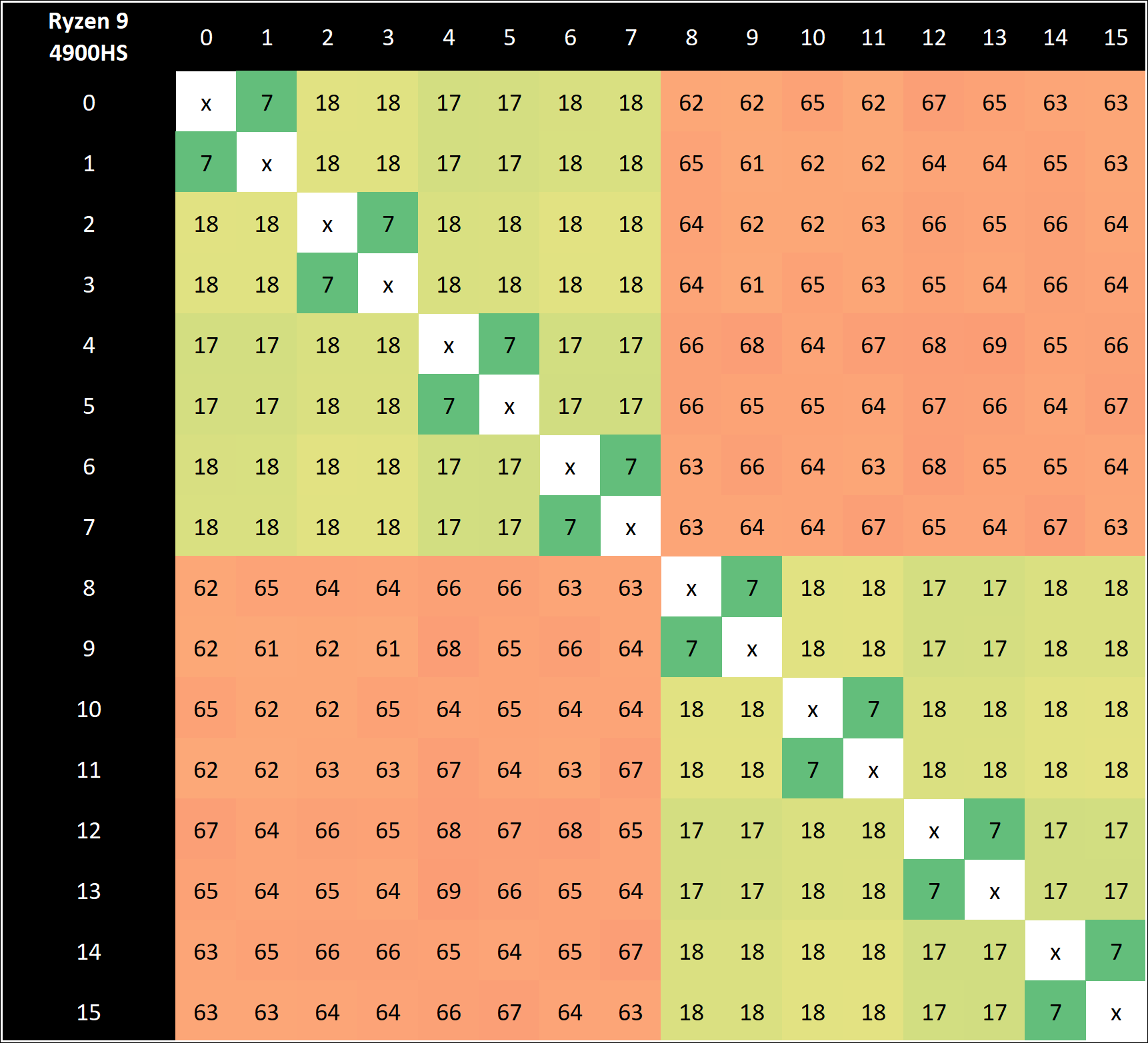
With our 4900HS, we have a 7 nanosecond latency for multithreads pinging inside a core, 17-18 nanosecond latency for threads within a CCX, and a 61-69 nanosecond latency moving across each CCX.
For a Ryzen 9 3950X, with two chiplets, the diagram looks a bit different:
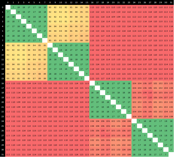
Here we see the same 7 nanoseconds for inside a core, 17-18 nanoseconds between cores in the same CCX, but now we have 81-89 nanoseconds between CCXes in the same chiplet, because we have to go off silicon to the IO die and back again. Then, if we want to go to a CCX on another chiplet, it can take 110-118 nanoseconds, because there’s another hop inside the IO die that needs to occur.
(AMD makes a thread leave the chiplet, even when it’s speaking to another CCX on the same chiplet, because that makes the control logic for the entire CPU a lot easier to handle. This may be improved in future generations, depending on how AMD controls the number of cores inside a chiplet.)
Going back to the Renoir CPU, we can compare this to the Intel Core i7-9750H in our Razer Blade machine:
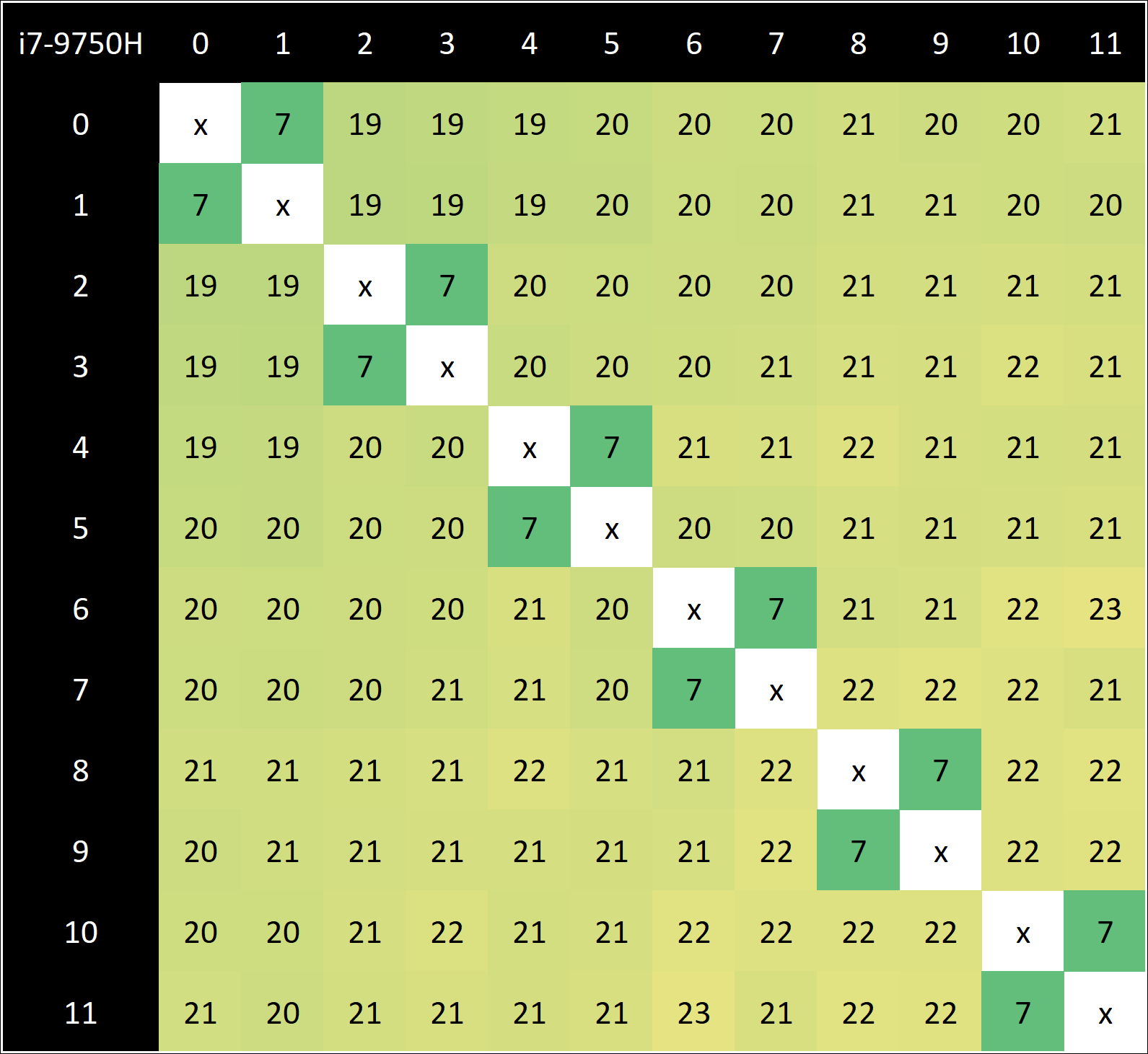
For the Core i7, we see a similar 7 nanosecond latency for a hyperthread, but in order to access any of the other six cores, it takes 19-23 nanoseconds. This is a tiny bit longer than AMD inside a CCX, because the Intel methodology is a ring-based topology, but Intel has the benefit of it being uniform across the whole chip, enabling the performance to be more consistent as the CPU has an effective homogenous latency. Intel’s ring topology is core count dependent, so more cores means a larger ring and a longer latency, but the variability of the ring becomes bigger (and less power efficient) when the ring gets bigger – this is why we saw dual ring designs in high-core-count Xeon chips for pre-Skylake.
Caching
For Renoir, AMD decided to minimize the amount of L3 cache to 1 MB per core, compared to 4 MB per core on the desktop Ryzen variants and 4 MB per core for Threadripper and EPYC. The reduction in the size of the cache does three things: (a) makes the die smaller and easier to manufacture, (b) makes the die use less power when turned on, but (c) causes more cache misses and accesses to main memory, causing a slight performance per clock decrease.
With (c), normally doubling (2x) the size of the cache gives a square root of 2 decrease in cache misses. Therefore going down from 4 MB on the other designs to 1 MB on these designs should imply that there will be twice as many cache misses from L3, and thus twice as many memory accesses. However, because AMD uses a non-inclusive cache policy on the L3 that accepts L2 cache evictions only, there’s actually less scope here for performance loss. Where it might hurt performance most is actually in integrated graphics, however AMD says that as a whole the Zen2+Vega8 Renoir chip has a substantial uplift in performance compared to the Zen+Vega11 Picasso design that went into the Surface Laptop 3.
For our cache latency structure, we got the following results:
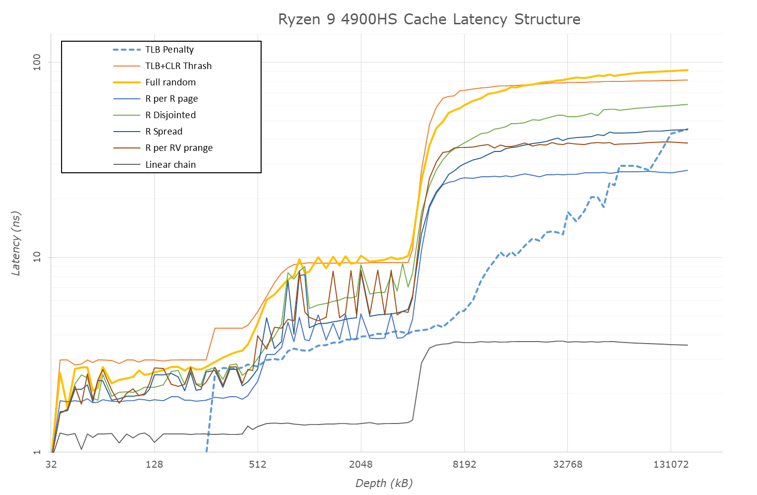
Our results show a worst case scenario with full random access latencies of
- 0.9 nanoseconds for L1 (4 clks) up to 32 KB,
- 3 nanoseconds for L2 (12-13 clks) up to 256 KB,
- 4-5 nanoseconds (18-19 clks) at 256-512 KB (Accesses starting to miss the L1 TLB here)
- 9.3 nanoseconds (39-40 clks) from 1 MB to 4 MB inside the rest of the CCX L3
- 65+ nanoseconds (278+ clks) from 6 MB+ moving into DRAM
It’s important to note that even though the chip has 8 MB of L3 total across the two CCX domains, each core can only access the L3 within its own CCX, and not the L3 of the other CCX domain. So while the chip is correct in saying there is 8 MB of L3 total, no core has access to all the L3. This applies to the desktop and enterprise chips as well (in case it wasn’t explicitly stated before).
Turbo Ramping
One of the key metrics of previous mobile designs is the ability for the core to jump from a low power state to a high power state very quickly, and then back down again. The faster you can do it, the better responsiveness for the user, but it also saves power by not keeping the high power state on for so long. It also helps that the processor ends up with a bunch of instructions to process, it can turbo up before they are finished, otherwise it wastes power doing the turbo for nothing.
For this test, we derive the frequency of a core at a microsecond level with instruction block throughput measurements while the CPU ramps up to its highest turbo state.
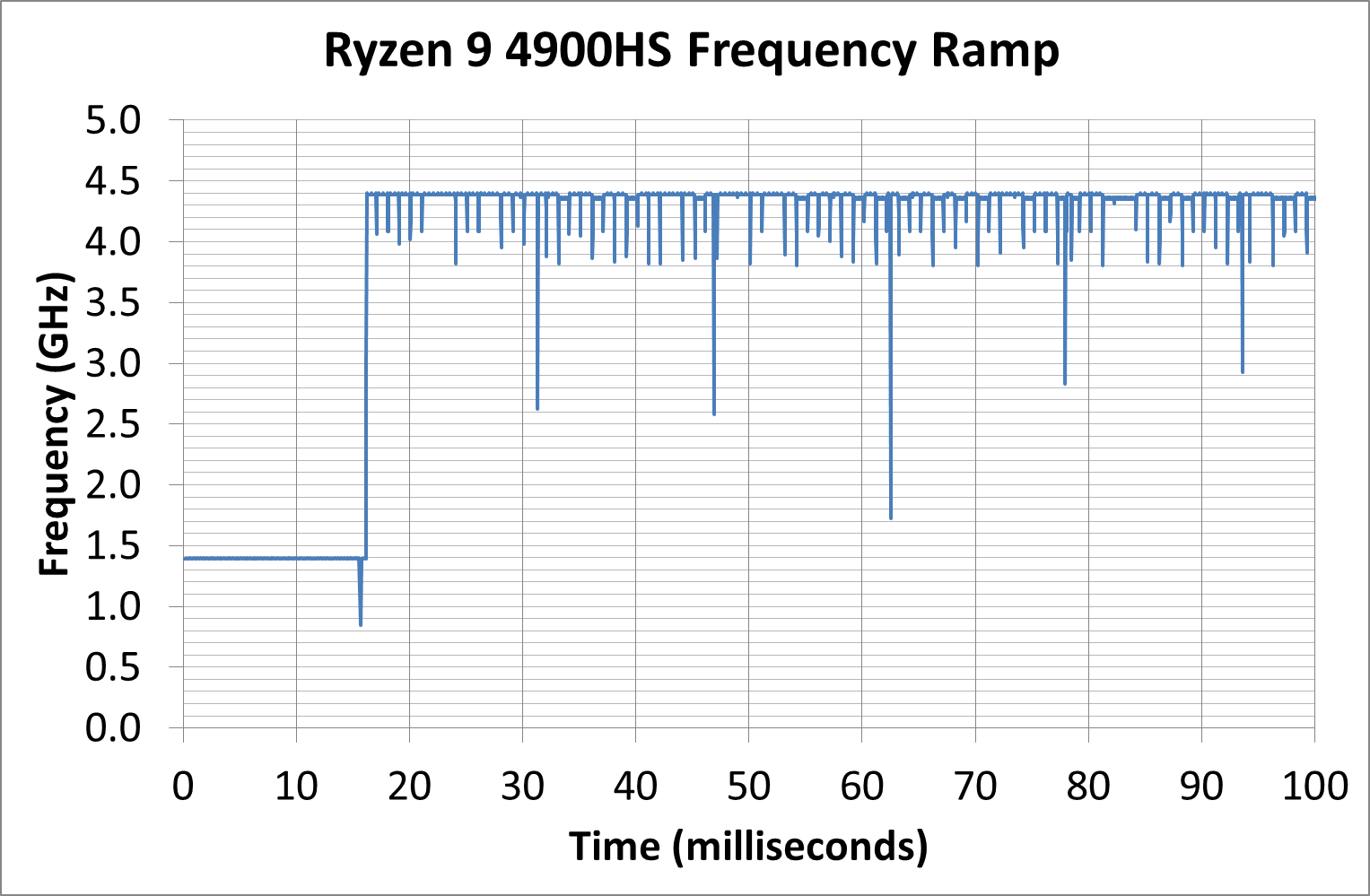
Here our Ryzen 9 4900 HS idles at 1.4 GHz, and within the request to go up to speed, it gets to 4.4 GHz (which is actually +100 MHz above specification) in 16 ms. At 16 ms to get from idle to full frequency, we’re looking at about a frame on a standard 60 Hz monitor, so responsiveness should be very good here.
We can compare this to the Core i7-9750H in the Razer Blade:
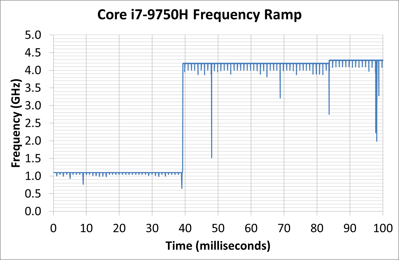
This processor idles a bit lower, at 1.1 GHz, and then gets to 4.2 GHz at around 39 milliseconds. The thing is though, this isn’t the top turbo frequency. Technically this CPU can get to 4.5 GHz, it even says so on the sticker on the laptop, however we see another small bump up to 4.3 GHz at around 83 milliseconds. So either way, it takes 2-4x longer to hit the high turbo for Intel’s 9th Gen (as setup by Razer in the Blade) than it does for AMD’s Ryzen 4000 (as setup by ASUS).


267 Comments
View All Comments
alufan - Friday, April 10, 2020 - link
As an it pro you should know betterhttps://www.amazon.co.uk/Anker-Ethernet-Including-...
Cooe - Thursday, April 9, 2020 - link
Because sticking a cheap USB adapter on the end of the Ethernet cable you plug into is just too much work? That problem is really minor to fix tbh.Icehawk - Sunday, April 12, 2020 - link
Agreed, for a home user - which this is aimed at I think it’s NBD but for enterprise machines I much prefer an integrated NIC so I don’t need to rely on a customer having a dongle (they won’t) or remembering to bring one. Sadly they are hard to find these days in this size laptop.At least this machine has a DIMM slot instead of soldered only.
GreenReaper - Monday, April 20, 2020 - link
Sure, but having to mod your memory because they didn't enable XMP profiles is not super-convenient. I'm sure Asus would like you to buy their RAM, but still. (Or perhaps it's an issue of Intel not giving the necessary data?)1_rick - Thursday, April 9, 2020 - link
What do you need a webcam for? I've seen a bunch of people here and at other sites call the lack of a webcam a hard pass.I use teleconferencing software extensively at my day job, both for meetings among people in different offices (and at home) and for meetings with clients, and nobody uses a webcam, although we're all far more interested in screen sharing, either to show someone how to do something, or to show a document of some kind, or whatever.
schujj07 - Friday, April 10, 2020 - link
^ThisTotally agree with this. I do the same thing and screen sharing is far more important for me in the IT world than a webcam. If you need a webcam go out and get a good one from Logitech instead of the included garbage on most laptops.
1_rick - Friday, April 10, 2020 - link
Yeah, that's the other thing--why wouldn't you want a better camera than the potato 720p you'll get with a laptop, if you do need one?haukionkannel - Saturday, April 11, 2020 - link
Webcams Are useful for personal contacts. At work I keep webcam mostly closed.And there Are/will be Also models with it, so people can chose what They pay for. So no worry if one Gaming laptop does not have it :)
Deicidium369 - Sunday, April 12, 2020 - link
People making imaginary purchases....sonny73n - Saturday, April 11, 2020 - link
That and privacy issue too. I have a piece of black electrical tape cover my laptop webcam. I would not know when it turns on by itself and snoops on me like those Samsung TVs a while back.The aholes would say I got something to hide. I would like to let them know that I’d rather break the law or break their faces than letting myself caught in my most embarrassing moments.