AMD Discusses ‘X3D’ Die Stacking and Packaging for Future Products: Hybrid 2.5D and 3D
by Dr. Ian Cutress on March 5, 2020 5:00 PM EST- Posted in
- CPUs
- AMD
- GPUs
- HBM
- TSMC
- Packaging
- AMD FAD 2020
- X3D
- Die Stacking
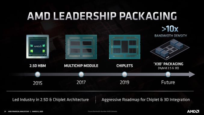
One of AMD’s key messages at its Financial Analyst Day 2020 is that the company wants to remain on the leading edge when it comes to process node technology as well as the latest packaging technology on its newest products. To that end, AMD discussed how it has surged forward with not only 2.5D interposer designs in its GPUs, but also stacked memory and chiplet implementations. The next stage of this journey, according to AMD, is a new X3D die stacking and packaging technology.
The nature of the Financial Analyst Day means that AMD didn’t go into too much detail here, aside from a few diagrams, but the company was clear that it sees its aggressive roadmap for chiplet and 3D integration to lead to this X3D design, where the X stands for ‘hybrid’. AMD’s diagrams show four main compute chiplets, arranged in a 2x2 pattern, and then 4-high stacked die with one per chiplet. All of these chips are then on a large interposer underneath.

Representation of AMD's diagram
In this case, it seems that the ‘die stacking’ element points to HBM or some form of memory, while the compute chiplets in the middle are only one high, but all connected through the interposer. AMD is claiming that this level of integration offers a 10x increase in bandwidth density, allowing more data to be shuttled from the memory stacks into the cores (and hopefully from storage into the memory stacks too).
The new packaging technology was listed as ‘future’, with no confirmed date. With AMD today announcing its new CDNA architecture for programmable compute graphics solutions, that sort of product would fit in really well here. With AMD’s prowess in CPU chiplet design, there could also be additional scope in future enterprise CPU developments as well. Graphics is a bit more farfetched, as the chiplet paradigm in graphics is a tricky one to solve.
We asked AMD more information about it, as to whether it correlates to any of TSMC’s latest packaging developments such as CoWoS or LIPINCON, however AMD stated that more would be detailed closer to the time at a dedicated event. We requested an AMD Architecture Day as soon as travel will allow. More to come as we find out about it.
Interested in more of our AMD Financial Analyst Day 2020 Coverage? Click here.


12 Comments
View All Comments
FreckledTrout - Thursday, March 5, 2020 - link
It's pretty obvious where things are headed and Nvidia should be scared. Honestly Intel and AMD are both going to have some very serious APU's in 5 years. When AMD is on TSMC's 3nm I really can see a 8-core chiplet, GPU chiplet, 32GB of HBM all on die. The densities that 3nm is slated to bring should make for iGPU's that rival even today's highest end dGPU's.IntelUser2000 - Thursday, March 5, 2020 - link
That's been said for years. One thing that won't change is cost of using stacked memory such as HBM2 and the power/thermal advantages of being a discrete GPU.All in all, it'll be like today with products largely differentiated by price and thermal envelope.
ChaosFenix - Friday, March 6, 2020 - link
So yes the costs of an interposer are relatively high in the consumer market but a design like this could shred data center loads. I will need to see it though. I think I have seen this rumor for a while.cb88 - Sunday, March 8, 2020 - link
And what costs would those be... and don't quote me the only numbers on the net because those are over 3 years old and were from an unreliable source even then.haukionkannel - Friday, March 6, 2020 - link
New games becomes more and more demanding... so some people there always will be room for discrete gpu. But to most common people... no need. Apu is enough.Smell This - Friday, March 6, 2020 - link
**We asked AMD more information about it, as to whether it correlates to any of TSMC’s latest packaging developments ...**______________________________________________
Well . . . . . DUH!
("Earth to Doc Ian . . . . Earth to Doc Ian")
;-)
Someguyperson - Thursday, March 5, 2020 - link
This looks pretty clearly like an enterprise compute card. It makes a ton of sense to produce cards like this for servers, but I'm not sure something this costly (and power dense) will make it into the consumer space for a while.Dragonstongue - Thursday, March 5, 2020 - link
Probably not likely any time soon, that being said AMD was clear on chiplet made it possible and was far far less expensive for them to be able to do, still turn a solid profit as well as being much easier to get pricing down far more quickly.I read this on a few different review sites thus far.
suppose it depends on what the chiplets are made for/what they will be doing, some losses, potential massive gains (in terms of latency chip-chiplet to the others)
With how "intelligent" these chips are these days, might be sooner and for a much smaller amount of $$$ to get into our hands...maybe somewhere along the line, SOMEONE, will be "wise" and say "let us start a "buy back" program, so we can salvage the costly materials, save the buyer some funds to have the latest and greatest and we now have "cream of the crop" recycled materials for our use again, why buy what we have already "consumed"
sort of speak.
probably help "tech wastelands" around the world from being toxified at least
schujj07 - Friday, March 6, 2020 - link
I could see this as a crazy enterprise CPU. Each chip having access to 32GB HBM3 @ ~1TB/sec bandwidth for an L4 style cache. The entire CPU package would be able to house an Oracle or MSSQL DB all in cache, SAP HANA not so much.Diogene7 - Friday, March 6, 2020 - link
I have some difficulties to understand why as of 2020, Intel, Qualcomm, AMD, Apple... are still not integrating the compute logic, the memory (ex: 12GB LPDDR5 DRAM), the storage (512GB Nand), all in one package, with an option to bypass any of those if a manufacturer wants to integrate more DRAM or storage ?Ideally also the wireless communication part (cellular (5G), WiGig 802.11ay, WIFI, Bluetooth, GPS,...) would be integrated in the same package.
All this would allow to have all essential building blocks to build ANY computer in one package, and hopefully with scale/volume, ultimately lower the cost down...