Amazon's Arm-based Graviton2 Against AMD and Intel: Comparing Cloud Compute
by Andrei Frumusanu on March 10, 2020 8:30 AM EST- Posted in
- Servers
- CPUs
- Cloud Computing
- Amazon
- AWS
- Neoverse N1
- Graviton2
Memory Subsystem & Latency
Memory performance in server chips is absolutely crucial due to the sheer core count in the system. Amazon’s Graviton2 chip has the most modern memory capabilities of our test set thanks to 8 DDR4-3200 memory controllers, providing up to a theoretical 204GB/s peak bandwidth. What’s also important, is the SoC’s cache hierarchy and the latencies it’s able to access data at.
Looking at the linear latency graph results, let’s first focus on the DRAM region and see how the Graviton2 ends up relative to the competition.

Surprisingly enough, the Graviton2 does extremely well. Although the cache hierarchies between the designs are very different, when looking at an arbitrary 128MB memory depth, the three systems are near identical. We do see that the Graviton2’s full random latency increases at a higher rate the deeper into DRAM you compare it against the AMD and Intel systems. The structural memory latency between the Amazon and AMD chips are near identical, meaning the AMD system doing better further down in random accesses probably is due to better TLBs or page-table walkers.

Our measured 81ns structural estimate figure here almost directly matches up with Arm’s published 83ns figure from a year ago, further giving credence to Arm’s published figures from back then (Arm's figure was LMBench random using hugepages, we're accounting for TLB misses in our patterns with 4KB pages).
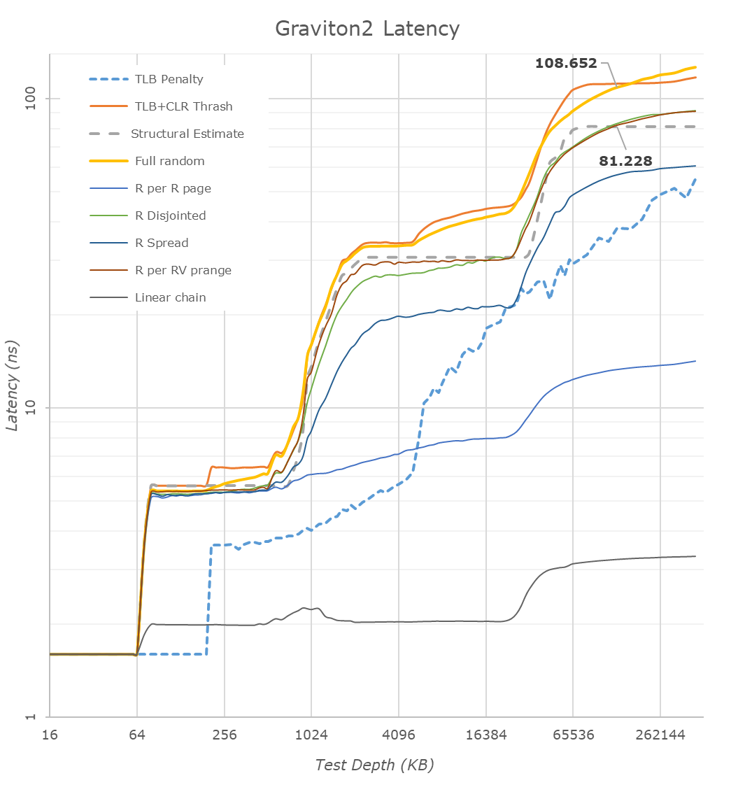
Turning to a logarithmical representation of the same data, we better see the difference in the cache hierarchy.
Compared to the AMD and Intel CPUs, we see the N1 cores’ advantage in the doubled 64KB L1D cache. Access latencies between the different cores should be 4 cycles, with the absolute figures in nanoseconds only differing due to the clock frequency differences between the cores.
The L2 cache of the Graviton2 falls in at 1MB and the access latency here is also competitive at 11 cycles. Arm gives the option between a 512KB 9 cycle or a 1MB 11 cycle configuration, and Amazon’s designers here chose the latter option. Halfway through the 1MB L2 cache we see the latencies of some access patterns increase, and this is due to the test exceeding the capacity of the L1 TLB which falls in at 48 pages (192KB coverage) for the N1 cores, also resulting in the big jump in the TLB miss penalty curve. AMD and Intel here go up to 64 pages and 256KB coverage. To be noted in these results is AMD’s prefetchers pulling into L2, whereas Arm and Intel cores only pull into L3 for more complex patterns.
Going beyond the L2, we reach the L3 where we’re able to test Arm’s CMN-600 mesh interconnect for the first time. The cache hierarchy covers 32MB depth; the interesting aspect here is that the latency remains relatively flat and within 2ns when testing some patterns between 3MB and 32MB, meaning there's fine-grained access hashing across the chip's slices.
The average estimate structural latency of the cache falls in at around 29.6ns, which isn’t all too great when compared to Intel’s ~18.9ns L3 cache, even considering that this is split up across 32 slices versus Intel’s 24 slices. Of course, AMD’s L3 leads here at only 10.6ns, but that’s only shared within 4 CPU cores and doesn’t go nearly as deep.
What we’re also seeing here is that the Graviton2’s N1 cores prefetchers aren’t set up to be nearly as aggressive in some more complex patterns than what we saw in its mobile Cortex-A76 siblings; it’s likely that this was done on purpose to avoid unnecessary memory traffic on the chip, as with 64 cores you’re going to be very bandwidth starved, and you don’t want to waste any of that on possible mis-prefetching.

Moving onto bandwidth testing, we’re solely looking at single-core bandwidth here.
Things are looking massively impressive for the Graviton2’s Neoverse N1 cores as a single CPU core is able to stream writes at up to 36GB/s. What interesting here is that the N1 cores like the Cortex-A76 cores here take advantage of the relaxed memory ordering of the Arm architecture to essentially behave the same as non-temporal writes would on an x86 system, and that’s why the bandwidth if flat across the whole test depth.
Loading from memory achieves up to 18.3GB/s and memory copy (flip test) achieves an impressive 29.57GB/s, which is more than double what’s achieved on the AMD system, and almost triple the Intel system. From a single-core perspective, it seems that the Arm design is able to have significantly better memory capabilities.
We’re still seeing the odd zig-zagging behaviour in the L1 and L2 caches for memory copies that we saw on mobile A76 based chips, possibly cache bank access conflicts for this particular test that showcase in Arm's new microarchitecture.
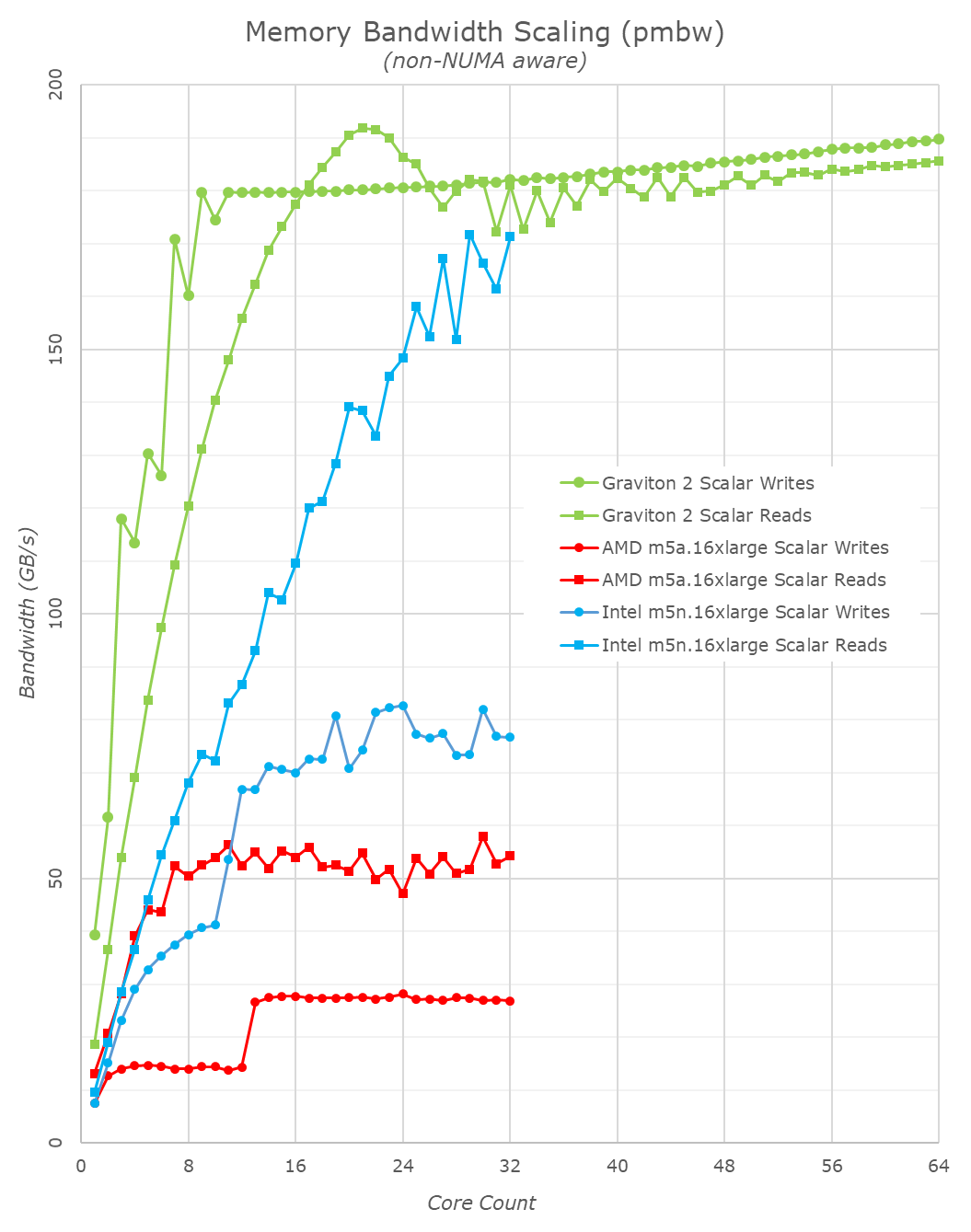
I didn’t have a proper good multi-core bandwidth test available in my toolset (going to have to write one), so fell back to Timo Bingmann’s PMBW test for some quick numbers on the memory bandwidth scaling of the Graviton2.
The AMD and Intel systems here aren’t quite representative as the test isn’t NUMA aware and that adds a bit of complexity to the matter – as mentioned, we’ll need to write a new custom tool that’s a bit more flexible and robust.
The Arm chip is quite impressive, and we only seemingly needed 8 CPU cores to saturate the write bandwidth of the system, and only 16 cores for the read bandwidth, with the highest figure reaching about 190GB/s, near the theoretical 204GB/s peak of the system, and this is only using scalar 64B accesses. Very impressive.


96 Comments
View All Comments
notladca - Tuesday, March 10, 2020 - link
I would love to know if the product line has split within Annapurna. In other words whether Graviton2 has, like previous Annapurna SoCs, some interesting support around storage and networking for use in future Nitro. It's possible Amazon has some behind the scenes work going on with CCIX for future machines. For example integrating their Inferentia chip more closely with the SoC.Given the core count, it'd also be interesting to compare ML inference acceleration via fp16 and int8 dot product instructions per core vs use of GPU or Inferentia.
coder543 - Tuesday, March 10, 2020 - link
One small bit of feedback: with that CPU topology chart, the coloration seems a little off. A difference of +/- 1 yields very different shades of red and orange, but the same difference on the green side of the spectrum yields no discernible difference in color? Personally, I think all of the 200 +/- 5 values in the first topology chart should be an almost uniform sea of orange/red. The important thing is the 150 difference in latency, not the +/- 1 latency, and the noise in the colors distracts the reader from the primary distinction. A lower signal to noise ratio.Also: what is the unit? nanoseconds? microseconds? milliseconds? I can’t figure it out, and it’s not labeled as far as I can tell.
Andrei Frumusanu - Tuesday, March 10, 2020 - link
Nanoseconds, I'll add a remark.sing_electric - Tuesday, March 10, 2020 - link
My tin hat is telling me to be suspicious of Amazon's pricing here. When shopping for cloud computing, perf/$ becomes VERY alluring, but I have to wonder if Amazon is willing to let its Gravitron servers be a "loss leader," artificially lowering prices to get market share until Arm on server is well-established - before then raising prices to something closer to a economically sustainable number.Andrei Frumusanu - Tuesday, March 10, 2020 - link
Vertical integration is powerful. Amazon can share profits and margins division wide, not having to pay overhead to AMD/Intel.sing_electric - Tuesday, March 10, 2020 - link
True, but then Amazon has to pay for the ARM license and 100% of the development/production costs. I would be very surprised if they managed to *make money* on the 1st couple Graviton generations (especially if you factor in having to buy Annapurna), since you'd need to say "of the $X generated by Graviton metal, $Y would have been spent on EC2 anyways, meaning $Z is our actual gain," and that's... probably too much to ask at this stage.rahvin - Tuesday, March 10, 2020 - link
The costs you mention are nothing compared to what they pay right now with Intel or AMD with they 50% margins on top of the actual cost. IMO this initiative was born out of Intel's price increases from 2010 to now. By vertically integrating they have full control over the price structure and they have very good data on what kind of workloads are running so they can tailor the design.IMO it was just a question of time until Amazon tried to vertically integrate this like they've done with shipping and lots of other stuff. Bezos is following the Robber Barron growth model.
dotjaz - Wednesday, March 11, 2020 - link
Huh? AMD has a gross margin of 40%, true. But keep in mind AWS has a operating margin of 30%, that mean AWS has a even higher gross margin than AMD, comparable to AMD's server department.Do you know what that means? For $1 of expenditure in to chip manufacturing, AWS expects to earn as much as AMD does. And since AWS don't have the volume as far as chip goes, their gross margin for chip investment will be lower, therefore not worth the investment if the decision is purely financial.
But yes, the other point stands, AWS have better control of costing (with more leverage as well) and performance.
Wilco1 - Wednesday, March 11, 2020 - link
For every $1 worth of silicon you could pay AMD $1.50, pay Intel $2 or pay TSMC $1 plus $0.20 internal development costs. Which works out best you think?extide - Friday, March 13, 2020 - link
It's not that simple. AMD and Intel can spread those development costs over vastly more processors. I mean we'll never know how it truly breaks down -- but I'd imagine Amazon has figure this all out and this will be pretty profitable for them.