Intel's Pentium 4 570J - Will 3.8GHz do the trick?
by Anand Lal Shimpi on November 14, 2004 10:56 AM EST- Posted in
- CPUs
Testing EDB Functionality
As we just mentioned, Intel’s Execute Disable Bit is enabled through Windows XP Service Pack 2, but being proponents of testing as many supported features as possible we turned to Robert Schlabbach’s Data Execution Prevention Test (aka NXTEST) to test Intel’s EDB.
CPUs that support Data Execution Prevention (DEP) will have to run in Physical Address Extension mode in order to enable DEP support. You can confirm the operating status by looking at the System Properties control panel:
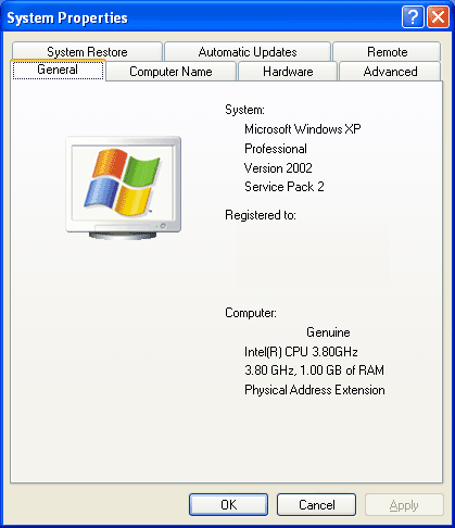
Physical Address Extension should be listed here.
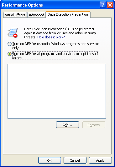
Before setting up NXTEST you have to enable full Data Execution Prevention under SP2. By default DEP is only enabled for certain Windows programs and services, given that NXTEST is not one off those Windows programs and services we had to manually enable DEP for all programs.
Microsoft buries the DEP controls under the Performance Options control panel, to get there you must first visit the System Properties control panel:
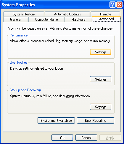
Then click on the advanced tab and select the Performance Settings option.
The third tab in the Performance Options control panel is the Data Execution Prevention tab, which is where you can enable/disable system-wide DEP:
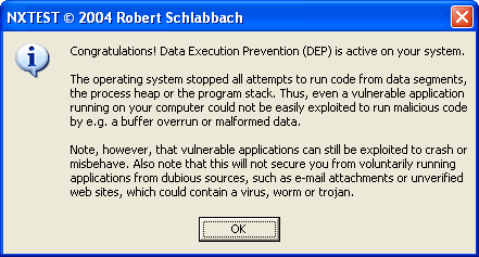
A reboot later we were ready to run NXTEST:
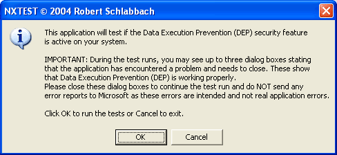
As expected, running the test confirmed that Intel’s EDB was working properly:
Intel didn’t make a huge deal out of EDB support for two likely reasons: 1) AMD beat them to the punch with their NX bit support, and 2) the benefits are not as tangible to end users since EDB doesn’t prevent all types of malicious code from wreaking havoc on your system, neither Intel nor AMD wish to inspire false confidence in their processors’ abilities to provide greater security.


42 Comments
View All Comments
Dustswirl - Sunday, November 14, 2004 - link
Aha! Thx guys!michaelpatrick33 - Sunday, November 14, 2004 - link
I meant #8 not #6 for the above post sorrymichaelpatrick33 - Sunday, November 14, 2004 - link
#6 You are right probably since they didn't mention 754 and that would give more parameters for the test. Good catch. They simply downclocked the 130nm 939 3500+.Glassmaster - Sunday, November 14, 2004 - link
#6: I'm pretty sure they downclocked a 130nm 939 3500+ for those measurements.Glassmaster.
Dustswirl - Sunday, November 14, 2004 - link
Quote:"[...]We also included power consumption figures from 130nm Socket-939 Athlon 64 3200+ and 3000+ chips, which as you may know, do not exist.[...]"
Mea culpa...
Dustswirl - Sunday, November 14, 2004 - link
Hmmmm so 2CH isn't like dual channel or? coz afaik 754 is single channel!Thx for the info :)
michaelpatrick33 - Sunday, November 14, 2004 - link
#4. They are using the 754 130nm core 3000+. That is why they say 90nm beside the 3500+ and not any of the other AMD64'sDustswirl - Sunday, November 14, 2004 - link
I don't understand how the A64 3500 90nm consumes less power then the A64 3000 (512/2CH) that is supposed to be also a 90nm part...michaelpatrick33 - Sunday, November 14, 2004 - link
The power consumption at load is a tad high for the 3.8 at being nearly twice as high as the 3500+. 226 vs. 114. That trend is obviously why Intel killed the 4.0 and beyond and the Tejas I would imagine. I wonder how much the 600 series chips from Intel will be with the extremely expensive L2 cache vs the current 3.6 and 3.8 chips.AtaStrumf - Sunday, November 14, 2004 - link
I've probably said this before, but I really like those tables with % numbers. You might wonna switch everything over to it. It gives a much more precise picture of diffence than those graphs.