FIRST LOOK - nForce4: Gigabyte K8NXP-9
by Wesley Fink on November 12, 2004 8:00 PM EST- Posted in
- Motherboards
Basic Features
| Gigabyte K8NXP-9 Specifications | |
| CPU Interface | Socket 939 Athlon 64 |
| Chipset | nVidia nForce 4 Ultra (Single-Chip) |
| Bus Speeds | 200MHz to 400MHz* |
| PCI Express Speeds | None in Pre-Release BIOS* |
| Core Voltage | 0.8V to 1.7V in 0.025V increments |
| CPU Clock Multiplier | 6x-25x in 1X increments* |
| HyperTransport Frequency | 1000MHz (1GHz) |
| HyperTransport Multiplier | 1X, 2X, 3X, 4X, 5X |
| DRAM Voltage | 2.5V to 3.1V in 0.1V increments* |
| HyperTransport Voltage | Normal, + 0.1V, +0.2V, +0.3V |
| Memory Slots | Four 184-pin DDR DIMM Slots Dual-Channel Configuration Regular Unbuffered Memory to 4GB Total |
| Expansion Slots | 1 x16 PCIe Slot 2 x1 PCIe Slots 3 PCI Slots |
| Onboard SATA/SATA RAID | 8 SATA Drive Total 4 SATA 300 Drives by nForce4 (RAID 0, 1, 0+1, JBOD) Can be combined with IDE drives in RAID 4 SATA 150 Drives by Sil3114CT176 (RAID 0, 1, 0+1, JBOD) |
| Onboard IDE/IDE RAID | Two Standard ATA133/100/66 (4 drives) Drives may be as IDE RAID or combined with nF4 SATA drives in a RAID Array |
| Onboard USB 2.0/IEEE-1394 | 10 USB 2.0 ports supported by nForce4 2 Firewire 1394B by TI 46A9C3W |
| Onboard LAN | Dual Gigabit LAN On-chip Gigabit LAN by nF4/Cicada 8201 PHY PCI Express Gigabit LAN by Marvel 88E8053 |
| Wireless LAN | PCI 802.11b/g Wireless LAN Card Included |
| Onboard Audio | AC '97 2.3 8-Channel by Realtek ALC850 |
| BIOS Revision | Award GA-K8NXP-9 M01 11/02/2004 |
The shipping Gigabyte BIOS provided many of the options that you would expect on a top-line board, but several areas like clock frequencies, memory voltage, and CPU ratios were very limited in the pre-release BIOS. The values reported in the chart above are the values that Gigabyte has assured us will be available in the production BIOS. These are much better ranges than those seen on recent Gigabyte boards. Most Enthusiasts will find these ranges very useful in tweaking the Gigabyte for top performance. As is Gigabyte custom in recent designs, Advanced Chipset Features (and Memory Timings) can only be seen when you press CTRL+F1 while in the BIOS.
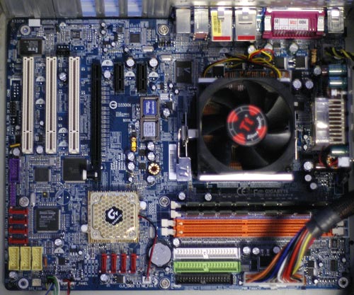
The Gigabyte K8NXP-9 was designed as a top-of-the-line nForce4 motherboard. As the flagship model, it sports all the top Gigabyte features. This starts with the DPS daughter card that you can see on the right of the board picture. This is used to increase power reserves and stability by increasing the board to 6-phase power. You will also see dual BIOS chips to the right of the PCIe x16 video slot. This trademark Gigabyte feature provides back-up BIOS in the event of a bad flash or unstable BIOS setting. The K8NXP-E can boot from the good backup BIOS if problems arise with the main BIOS.
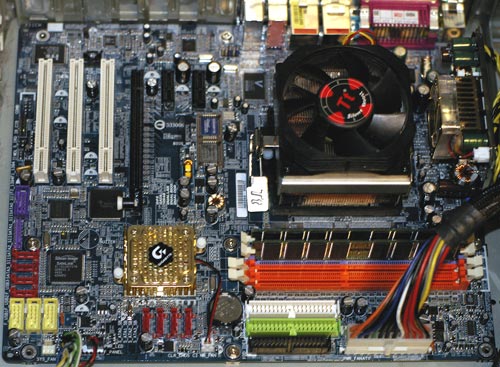
An analysis of board layout is beyond the scope of a First Look, but there are several things that stand out on the Gigabyte. Power connectors are ideally located on board edges in reasonable locations. This will be appreciated by anyone who has tried to snake these bulky cables around a CPU or fan. The floppy and IDE connectors are also ideally located on the far right edge of the board above the midline. Ports are concentrated at the bottom of the board, out of the way of the PCI and PCIe slots.
Continuing the theme of "more than you might expect", Gigabyte provides eight SATA ports. Four ports are 3Gb/s ports provided by the nForce4 chip, and four ports are 1.5Gb/s ports driven by the PCI bus. The 2nd group of ports is useful, but they would have been much more exciting if they had been 3Gb/s ports like those provided by nForce4.
Probably the most significant upgrade from the nF3 Ultra Gigabyte is the decision to adhere to nVidia's feature set. This time, we see Gigabyte use the nF4 on-chip Gigabit LAN by supporting it with a Vitesse (Cicada) Gigabit PHY. In fact, Gigabyte went one step further by including a second Gigabit LAN on the PCI Express Bus. This second on-board LAN is also removed from the constraints of the slower PCI bus since it resides on the much faster PCIe bus. For those using wireless networks there is a even a third option as Gigabyte includes a PCI 802.11 b/g card in the package.
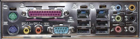
Audio is AC '97 2.3, but Gigabyte uses the popular 8-channel Realtek ALC850. The K8NXP-9 includes a wide range of audio I/O to make the most of the 850 chip. This includes 6 programmable audio mini-jacks and coax SPDIF in and out - all on the rear panel. There is more information on the Realtek 850 at the Realtek web site for those who are interested.
Another pioneering feature for Gigabyte has been their support of 1394B Firewire on their boards. This continues with the K8NXP-9 with 2 ports capable of 800MB/s. This is double the speed of 1394A for those looking for fast Firewire access.


49 Comments
View All Comments
arswihart - Saturday, November 13, 2004 - link
quote by Wesley Fink:"#6 - Full performance comparisons of nForce3 Ultra and nForce4 were run at nF4 launch at http://www.anandtech.com/cpuchipsets/showdoc.aspx?... Performance of nF3 and nF4 is basically the same - the only real difference is PCIe instead of AGP."
but you are showing here that the production board from Gigabyte is a little different than the reference nf4 boards. I think it would be helpful to at least include one good nf3-250gb board in some future nf4 round-up or review, for comparison's sake, as i think its more practical at this point to compare nf3 to nf4, rather than reference nf4 to production nf4.
Thanks for the review though, and I'm also interested in the price of these nf4 boards. I've seen somewhere quoting these boards on average at like $180
Whizzmo - Saturday, November 13, 2004 - link
Possible Typo:Page 2, below the second mobo pic, the following:
Four ports are 3Gb/s ports provided by the nForce3 chip, and
should probably be:
Four ports are 3Gb/s ports provided by the nForce4 chip, and
Danke :)
johnsonx - Saturday, November 13, 2004 - link
oh, ok... 1.5Gbps and 3Gbps signalling rates, which translate down to 150MB/s and 300MB/s data rates, respectively. The SATA uses 8b/10b encoding, so 10 bits of signalling are need for each 8 bits of data.Anyway, nevermind.
johnsonx - Saturday, November 13, 2004 - link
ok, it's late, so I may be tired and crazy....but what's all this about 1.5Gb SATA and 3Gb SATA? I thought standard SATA is 150MB/s (SATA-150), while the new SATA 2.0 spec runs at 300MB/s. Even converting those speeds to Gigabits per second, you get 1.2Gbs and 2.4Gbps.
Jalf - Saturday, November 13, 2004 - link
Would be nice to see it compared to ATI's A64 board. That looked like a pretty good performer as wellstelleg151 - Saturday, November 13, 2004 - link
Any clues as to when we will be able to get our hands on one?RyanVM - Saturday, November 13, 2004 - link
Too bad the secondary SATA controller isn't on the PCIe bus.xtknight - Saturday, November 13, 2004 - link
wow, very interesting. looks like the gigabyte mobo is a winner. by the way, doom 3 belongs under OpenGL benchmarks.PorBleemo - Friday, November 12, 2004 - link
So much for that "Fatal1ty". :PProviaFan - Friday, November 12, 2004 - link
Page 2 "Four ports are 3Gb/s ports provided by the nForce3 chip"Oops?