Analyzing Intel’s Discrete Xe-HPC Graphics Disclosure: Ponte Vecchio, Rambo Cache, and Gelato
by Dr. Ian Cutress on December 24, 2019 9:30 AM ESToneAPI: Intel’s Solution to Software
Having the hardware is all well and good, but the other angle (and perhaps more important angle) is software. Intel is keen to point out that before this new oneAPI initiative, it had over 200+ software angles and projects across the company to do with software development. oneAPI is meant to bring all of those angles and projects under one roof, and provide a single entry point for developers to access whether they are programming for CPU, GPU, AI, or FPGA.
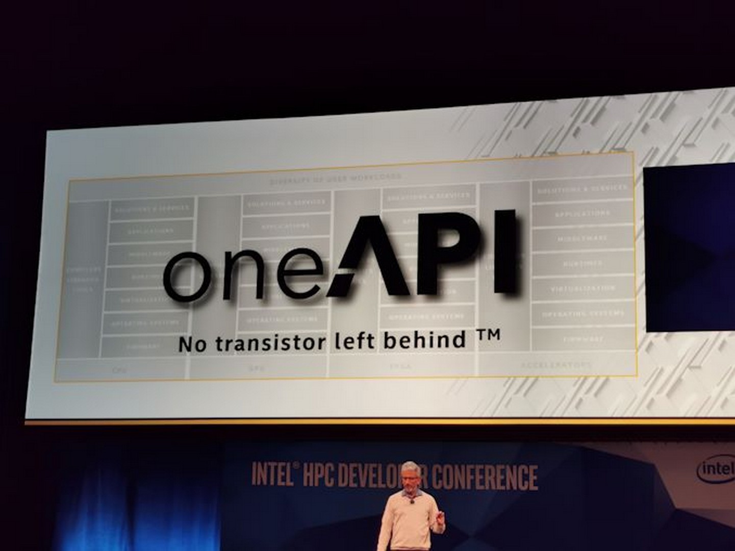
The slogan ‘no transistor left behind’ is going to be an important part of Intel’s ethos here. It’s a nice slogan, even if it does come across as if it is a bit of a gimmick. It should also be noted that this slogan is missing a key word: ‘no Intel transistor left behind’. oneAPI won’t help you as much with non-Intel hardware.
This sounds somewhat too good to be true. There is no way that a single entry point can do all things to all developers, and Intel knows this. The point of oneAPI is more about unifying the software stack such that high-level programmers can do what they do regardless of hardware, and low level programmers that want to target specific hardware and do micro-optimizations at the lowest level can do that too.
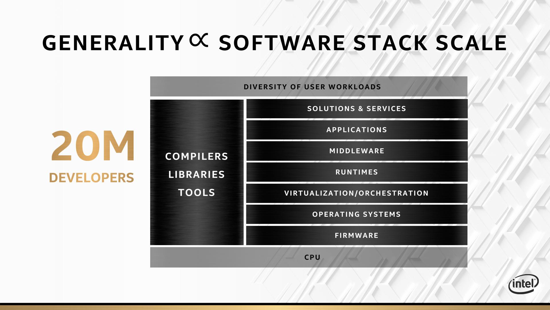
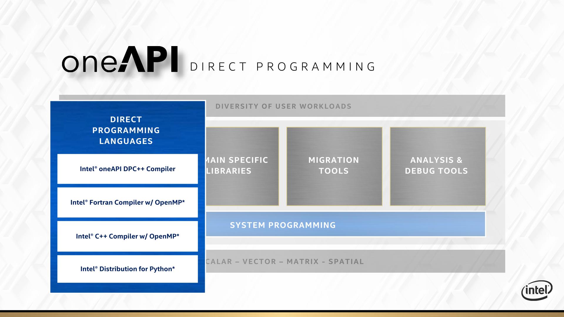
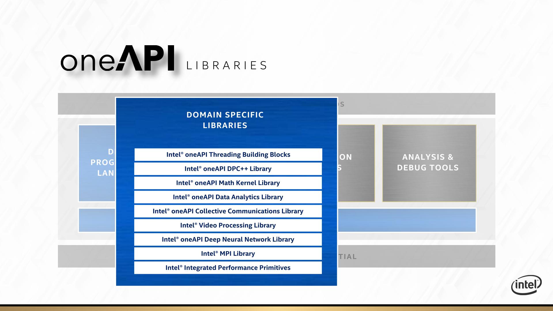
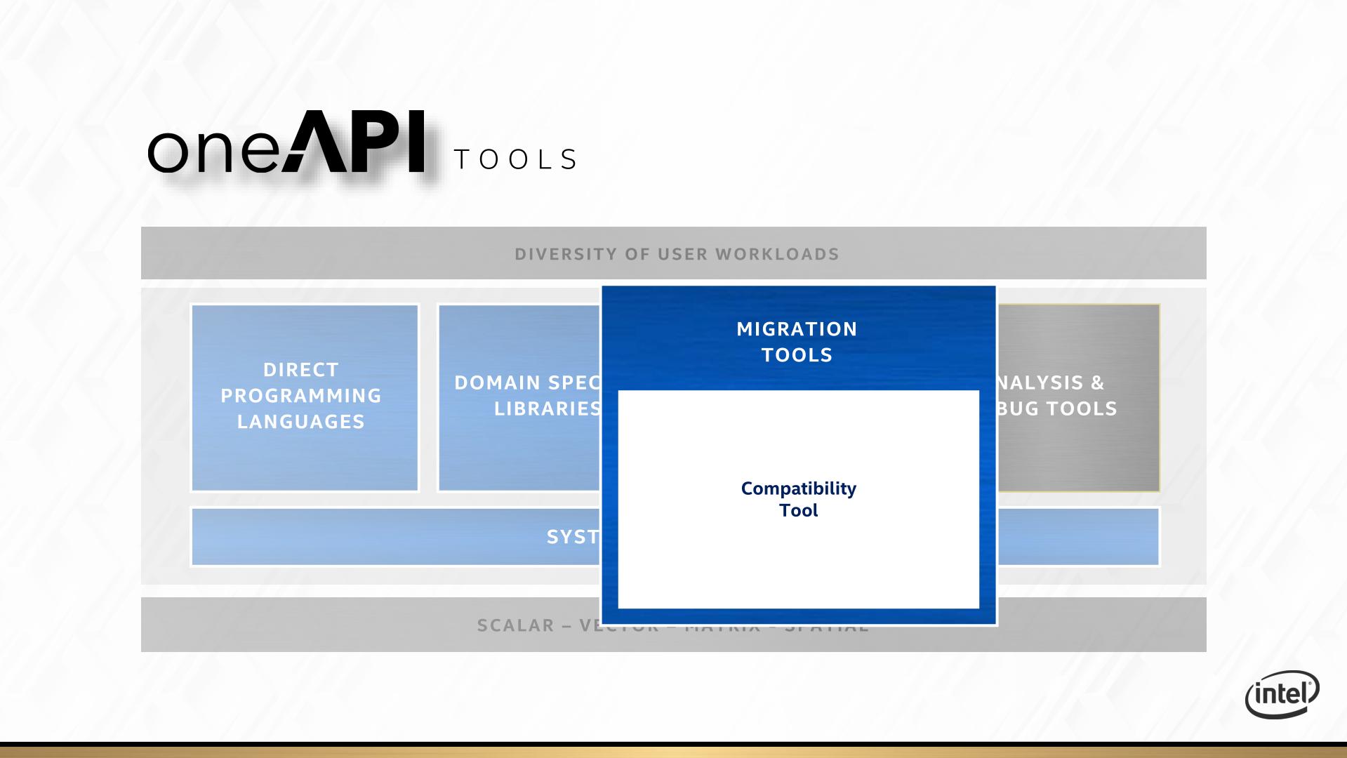
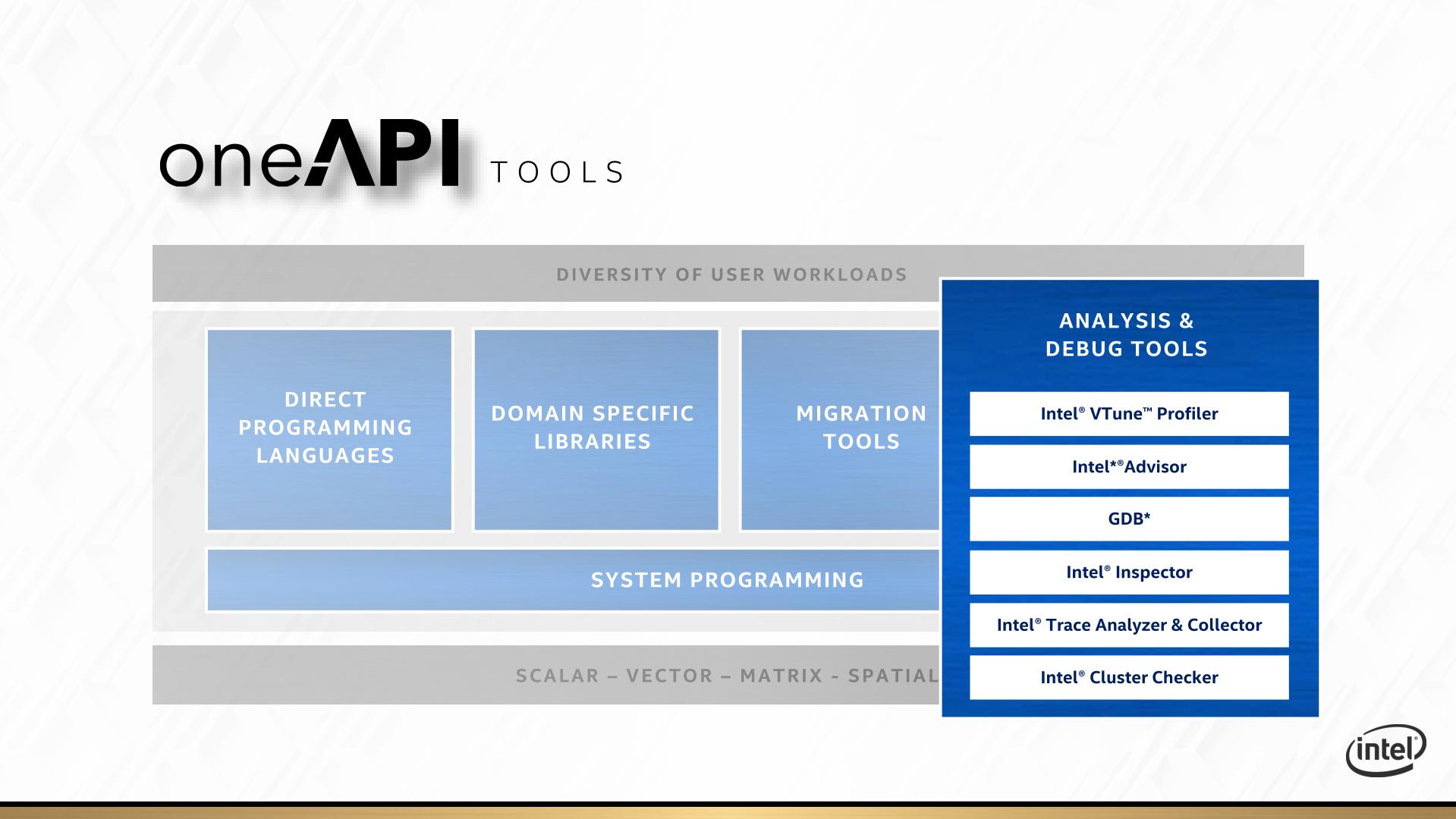
Everything for oneAPI is going to be driven through the oneAPI stack. At the bottom of the stack is the hardware, and at the top of the stack is the user workload – in between there are five areas which Intel is going address.
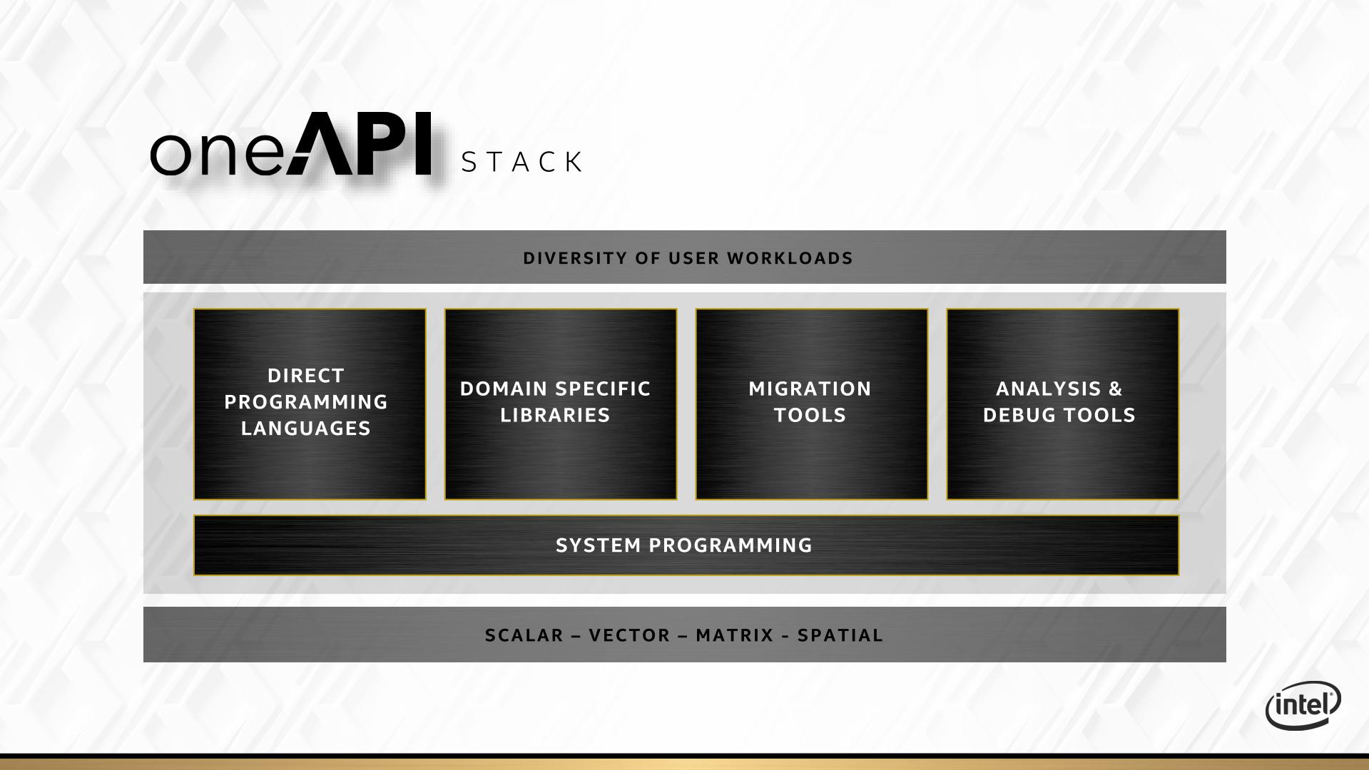
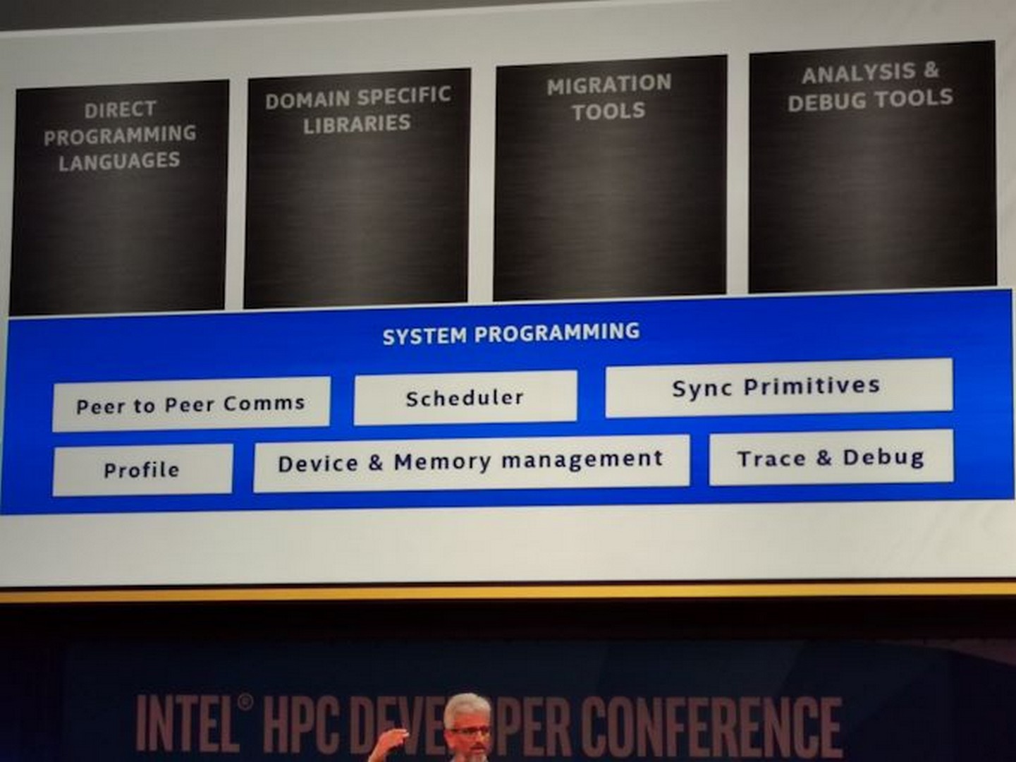
The underlying area that covers the rest is system programming. This includes scheduler management, peer-to-peer communications, device and memory management, but also trace and debug tools. The latter of which will appear in its own context as well.
For direct programming languages, Intel is leaning heavily on its ‘Distributed Parallel C++’ standard, or DPC++. This is going to be the main language that it encourages people to use if they want portable code over all different types of hardware that oneAPI is going to cover. DPC++ is an intrinsic mix of C++ and SYCL, with Intel in charge of where that goes.
But not everyone is going to want to re-write their code in a new programming paradigm. To that end, Intel is also working to build a Fortran with OpenMP compiler, a standard C++ with OpenMP compiler, and a python distribution network that also works with the rest of oneAPI.
For anyone with a categorically popular workload, Intel is going to direct you to its library of libraries. Most of these users will have heard of before, such as the Intel Math Kernel Library (MKL) or the MPI libraries. What Intel is doing here is refactoring its most popular libraries specifically for oneAPI, so all the hooks needed for hardware targets are present and accounted for. It’s worth noting that these libraries, like their non oneAPI counterparts, are likely to be sold on a licencing model.
One big element to oneAPI is going to be migration tools. Intel has made a big deal what they want to be able to support CUDA translation to Intel hardware. If that sounds familiar, it’s because Raja Koduri already tried to do that with HIP at AMD. The HIP tool works well in some cases, although in almost all instances it still requires adjustment to the code to get something in CUDA to work on AMD. When we asked Raja about what he learned about previous conversion tools and what makes it different for Intel, Raja said that the issue is when code written for a wide vector machine gets moved to a narrower vector machine, which was AMD’s main issue. With Xe, the nature of the variable vector width means that oneAPI shouldn’t have as many issues translating CUDA to Xe in that instance. Time will tell, for obvious reasons. If Intel wants to be big in HPC, that’s the one trick they’ll need to execute on.
The final internal pillar of oneAPI are the analysis and debug tools. Popular products like vTune and Trace Analyzer will be getting the oneAPI overhaul so they can integrate more easily for a variety of hardware and code paths.
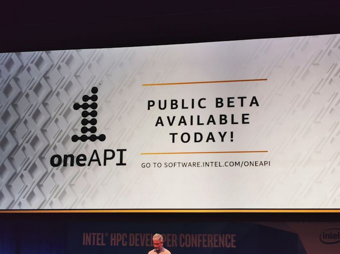
At the Intel HPC Developer Conference, Intel announced that the first version of the public beta is now available. Interested parties can start to use it, and Intel is interested in feedback.
The other angle to Intel’s oneAPI strategy is supporting it with its DevCloud platform. This allows users to have access to oneAPI tools without needing the hardware or installing the software. Intel stated that they aim to provide a wide variety of hardware on DevCloud such that potential users who are interested in specific hardware but are unsure what works best for them will be able to try it out before making a purchasing decision. DevCloud with the oneAPI beta is also now available.


47 Comments
View All Comments
MenhirMike - Tuesday, December 24, 2019 - link
This is way above the stuff I work with, but now I want RAMBO Cache on all my stuff.Batmeat - Tuesday, December 24, 2019 - link
How did he know I would do that?
Duncan Macdonald - Tuesday, December 24, 2019 - link
Given Intel's brilliant(!!!) success in getting its 10nm process to work, I would take the dates with a few megatons of salt!!!repoman27 - Wednesday, December 25, 2019 - link
Ian, I think your block diagram is a little off. Although the Intel illustrations clearly involve a certain amount of artistic license, I think we can agree that there's an organic package substrate with 8 HBM stacks and 2 transceiver tiles which are connected via EMIB to two larger modules. The modules appear to be a stack with two interposers sandwiched together. The bottom interposer has 8 large chips which are most likely the XeMF dies, as well as several color coded regions representing EMIB zones along with a bunch of vias. The top interposer has the 8 XeHPC chiplets and 4 additional chips which are almost certainly the RAMBO caches, seeing as they look exactly like the depiction of said caches in the other slide. Then there is one giant ball grid connecting the top and bottom layers of the sandwich.That looks an awful lot like Co-EMIB to me. The 7nm compute chiplets and SDRAM caches (built on whatever process is the best fit) are bonded directly (Foveros) to a wafer with the memory fabric dies (probably on 14nm) and riddled with TSVs. Those modules then get singulated and plunked onto a substrate with a bunch of EMIBs inserted into it which connect them to each other as well as to the HBM stacks and transceiver tiles.
Also, this point seems a little harsh: "Transition through DDR3 to DDR4 (and DDR5?) in that time frame". Intel may be way behind on their roadmap, but they made the transition to DDR4 several years ago with Skylake.
repoman27 - Wednesday, December 25, 2019 - link
In fact, Intel may have already shown off a prototype wafer of the modules themselves: https://pbs.twimg.com/media/D_C-9b3U0AAeyv7.jpgvia Anshel Sag on Twitter: https://twitter.com/anshelsag/status/1148627973882...
thetrashcanisfull - Wednesday, December 25, 2019 - link
This seems worryingly light on technical details with a lot of bold performance claims. Particularly the architectural stuffIf Intel really has managed to execute a proper chiplet style GPU with EMIB / chip stacking, that would certainly open the door to major performance uplifts, but they are staying super vague on the underlying architecture and topology. Honestly, this slideware feels reminiscent to 3D XPoint, which, while still a solid technology, was years late and never delivered on the sort of hype it was announced with.
I'll remain skeptical until we get more details - the advances in packaging and interconnects that Intel is touting could certainly enable improvements on this scale, but Intel's execution over the last decade leaves a lot of room for doubt.
smilingcrow - Wednesday, December 25, 2019 - link
'Intel's execution over the last decade leaves a lot of room for doubt.'Decade! I thought they were ahead of the pack generally until Zen 2 was released 18 months ago!
They have had a terrible 2 years but if you want to look at the last decade the real underachievers surely were AMD.
The next few years are crucial so we will have to see how things pan out.
thetrashcanisfull - Wednesday, December 25, 2019 - link
Decade may be an exaggeration, but not by much. Look at all of Intel's attempts to break into markets new markets: mobile/cellular, Larrabee/MIC, FPGAs (Altera), 3D XPoint...Intel has shown that it can be fairly successful as an incumbent in the server/desktop/laptop CPU market (or at least it could until the 10nm problems) but outside of that Intel has consistently struggled to deliver on anything over the last 8+ years.
jabber - Wednesday, December 25, 2019 - link
Maybe it could be said with AMD struggling they did let off the gas pedal a bit and coasted a while.thetrashcanisfull - Wednesday, December 25, 2019 - link
I think that's certainly true. Intergenerational improvements post Sandy Bridge were pretty anemic in the consumer market largely since intel refused to put out more than 4 cores on a mainstream platform until coffee lake. In the server/HEDT intel was doing pretty well for a while by virtue of increasing core counts, but the 10nm woes have halted any progress on that front.