Qualcomm Announces Snapdragon 865 and 765(G): 5G For All in 2020, All The Details
by Andrei Frumusanu on December 4, 2019 1:50 PM EST- Posted in
- Mobile
- Qualcomm
- Smartphones
- SoCs
- 7nm
- 5G
- Snapdragon 865
- Snapdragon 765
Immense AI, Camera and ISP Upgrades
New Hexagon 695 DSP: 4x Performance On New Tensor Cores - 15 TOPs Total on SoC
The Snapdragon 865 now ships with the new Hexagon 695 DSP block. The single biggest improvement of the new design is a massive quadrupling of the processing power of the dedicated tensor cores. This jump alone is able to double the SoC’s aggregate AI processing ability up from 7 TOPs to 15 TOPs.
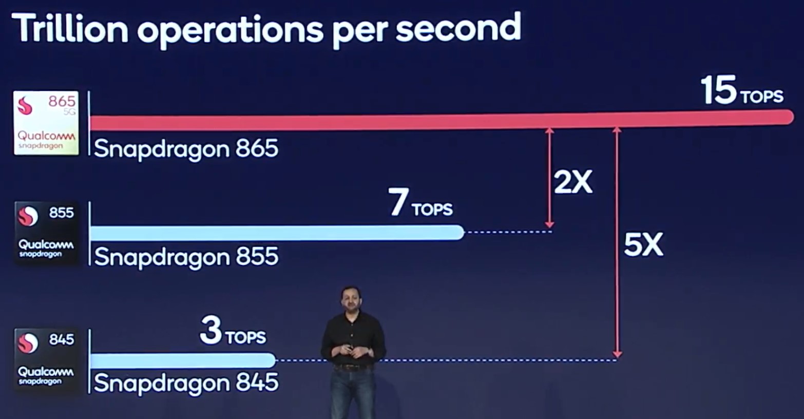
Qualcomm here still doesn’t properly do a breakdown between the IP blocks which contribute to this number, but given that the GPU only saw a ~20% increase, and that the Hexagon’s scalar and vector execution units this year have remained the same in terms of performance, we estimate that the tensor units now roughly come in at around 10TOPs by themselves.
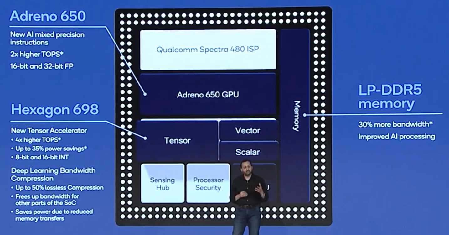
Qualcomm has also now included lossless weight and activation compression for the Tensor cores, being able to reduce bandwidth consumption up to 50%. This is a similar feature we've seen advertised by third-party NPU IP offerings, only that Qualcomm is going to be shipping this now in a product in just a few months.
Power efficiency of the block is also have said to have improved by 35%, making computations less costly in terms of battery life.
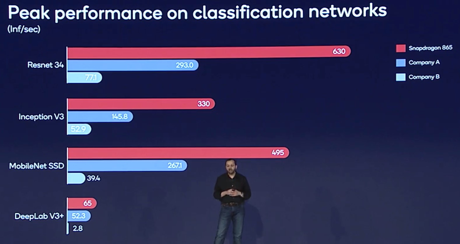
Qualcomm talks how about its inference performance and inference power efficiency is significantly higher than competing solutions. We don't know the comparison SoCs being showcased here, but a likely candidates here are the Apple A13 and the Kirin 990? It could also be an Exynos or other SoC.
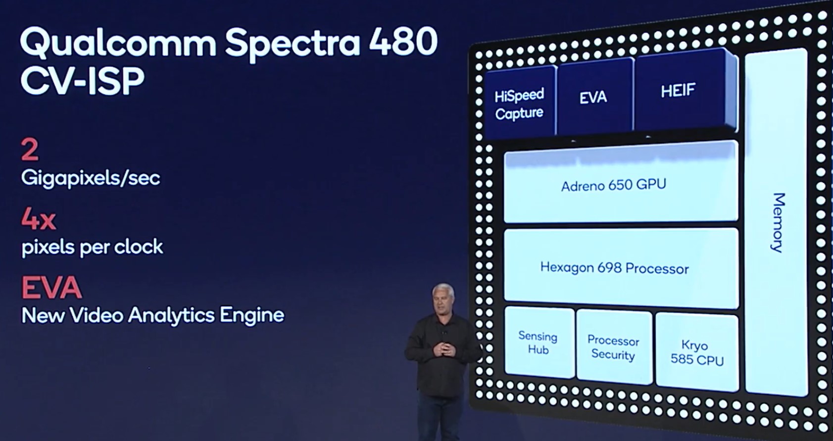
New Spectra CV-480 ISP: 2 Gigapixels/s Enabling Massive Sensors
Aside from its 5G abilities, it’s very much evident that camera is very much at the very centre of the Snapdragon 865’s new features. The whole camera subsystem has seen some massive upgrades in the IP, and amongst the biggest improvements in capability lies in the new Spectra 480 computer-vision ISP.
The new IP has seen a major architectural change in that it’s now able to process 4 pixels per clock instead of just only 1 PPC as in the previous generation. This has now massively upgraded the pixel processing throughput to 2 Gigapixels/second, allowing the SoC a wide variety of use-cases that in the past simply weren’t possible due to lack of raw power.
Starting off with video capture, the new SoC is able to now record in 4K HDR while simultaneously capturing up to 64MP still shots at the same time. But 4K video isn’t the limit anymore – and you even can say that in terms of framerate as now 4K120 recording is supported, but the Snapdragon 865 now supports 8K30 video recording.
Video recording quality continues to support all the features we’ve seen in the previous generation, meaning 10-bit and various HDR standards such as HLG, HDR10, HDR10+, but now the new SoC expands this even further with the introduction of the ability to do live recording in the Dolby Vision HDR standard. Qualcomm explains that the Snapdragon 865 not only is the first smartphone SoC to be able to do this, but it’s the first camera platform of any kind in the world, as usual Dolby Vision content right now is enabled post-capture in the editing room, rather being something that’s being natively recorded by a camera.
The new improved capabilities of the ISP and video encoder also erase some current recording limitations, for example, slow-motion video recording at 960fps is sustained indefinitely instead of being limited to a couple of seconds of real-time footage.
Although normally I wouldn’t have brought this up, MediaTek’s recent release of the Dimensity 1000 did recently popularise the discussion topic: No, the Snapdragon 865 doesn’t support the AV1 codec for video decoding. It looks like we’ll have to wait for the next generation for that.
In terms of still capture photography, the new ISP performance will now allow for support for sensors of up to 200MP, which actually don’t yet exist as Samsung’s recent 108MP behemoth is currently the largest of its class right now.
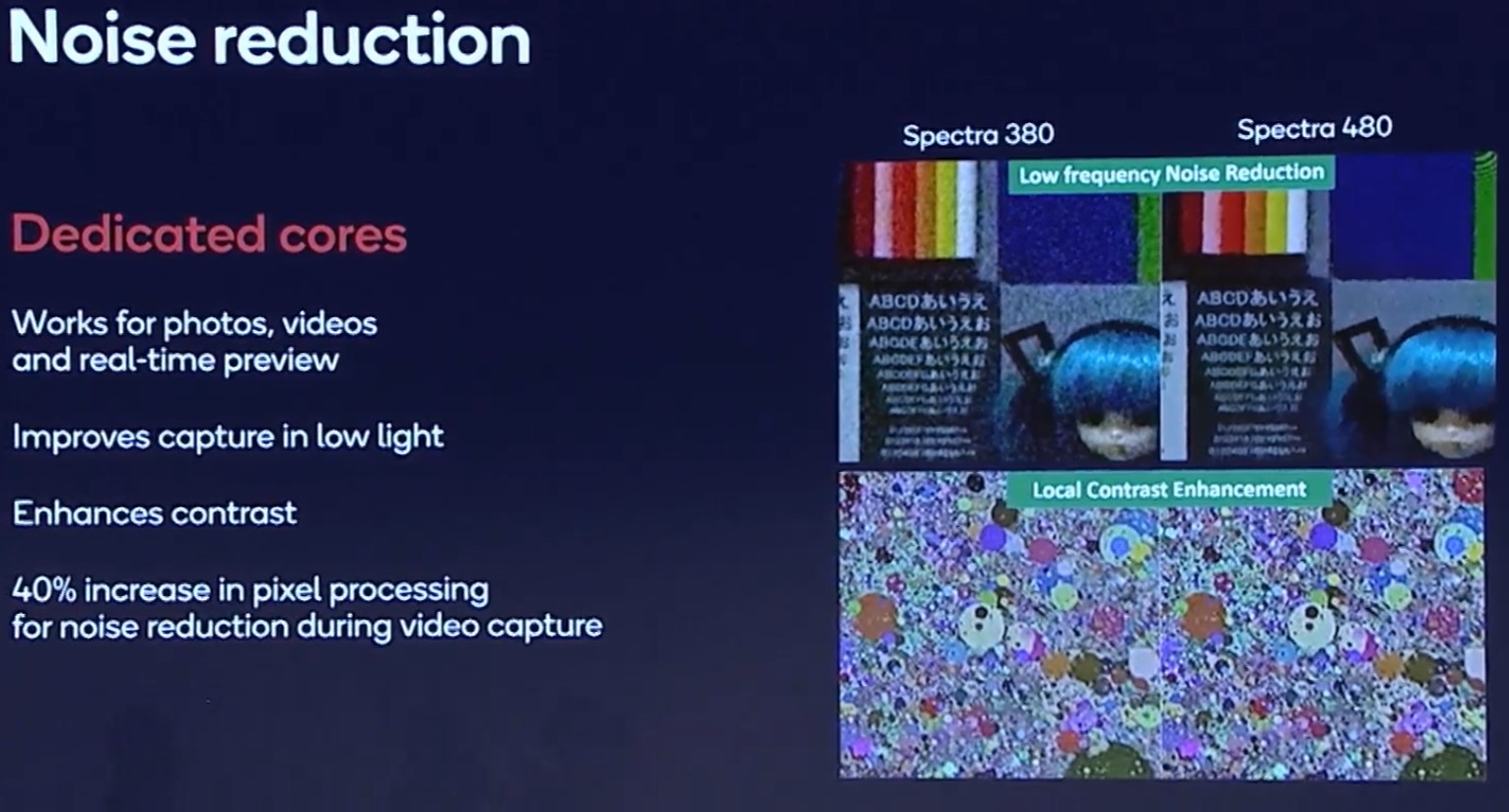
The new ISP now has various new functionalities in order to improve noise reduction and contrast enhancements. Particularly the new noise reduction features is said to be quite difficult to achieve.
Although Qualcomm advertises the 200MP figure predominantly, it’s to be noted that actual capture with zero shutter lag (ZSL) is limited to 64MP – so there is a rather larger compromise in capturing at resolutions beyond 64MP.
High Refresh Rate Displays Normalised: Support For 144Hz
Already some vendors are leading the pack in 2019, but we’re expecting 2020 to see wide-range adoption of high refresh-rate displays. Even more importantly, we’ll be seeing implementations at high resolutions higher than 90 and 120Hz, supporting up to 144Hz displays. Qualcomm explains that the barrier that’s been lifted here is the SoC’s Display Processing Unit (DPU) that has had its throughput significantly increased.
I asked the company about the impact on battery life and which component of a phone accounts for the highest power increases. Surprisingly, it’s not any one component, with most of them seeing pretty much just an evenly distributed linear increase in power requirements, with the actual display panel itself (excluding the DDIC), seeing actually the least increases in power draw.


91 Comments
View All Comments
generalako - Thursday, December 5, 2019 - link
I wonder. Wouldn't it be better to have 2 + 6 cores like Apple, rather than 4 large cores + 4 small cores? That way ARM could make their main Cortex Core wider and massively increase cache, which plays a large part in Apple's performance advantage.peevee - Thursday, December 5, 2019 - link
Apple does 2+4.6 A55s would not produce MT performance of 4 Apple Thunders though at energy-efficient frequencies.
I suspect with the right scheduler, something like 1+8 (or even 1+12) would be the best combination of ST and MT at any given TDP.
Especially if the small cores are redesigned to say share L1I cache (in MT-critical things they mostly run the same loops) and wide decoder and have L0I (microcommand cache) and L1D per core. Maybe even secondary expensive ALUs for superscalar execution (cheap ops like add/sub or logic can have 2-3 ALUs in each cores for the cost of only a few transistors).
Kangal - Saturday, December 7, 2019 - link
A better arrangement would be 3+5.Most applications are still threaded with "dual core" heirachy and few spilling over the "quad core" scheduling. So having a Third Large Core would keep the single core and dual core threads running well, whilst helping to smooth off those extra/stray threads.
The small cores are getting long in the tooth, and haven't had a decent upgrade since they were introduced back in 2015. Having the extra fifth core, and raising clocks would help slightly. But its no competition against Apple's Thunder Cores. To show you how impressive they really are, they are consuming (slightly) less than certain Cortex A55 cores whilst performing (slightly) faster than certain Cortex A73 cores.
ARM is already at the drawboard designing their next-generation architecture: ARM v9. So I suspect that's when we will see them leapfrog the competition in 2021-2022. I'm hoping for an APU design with a monolithic GPU at the centre, surrounded by a shared RAM, then chiplet CPUs, which are then surrounded by flash storage blocks and co-processors, with the I/O finally coming out from the SoC. That way they can scale it from 3W small-phones, to 5W large-phones, 7W tablets, 15W laptops, or even 45W for a Console/Desktop-like form factor.
Kabm - Thursday, December 5, 2019 - link
Apple advantage/disavantage is they cannot have modem intergrated so they have more room for cpu. Qualcomm don't have their own cpu core design anymore and they use ARM Cortex. ARM Cortex cores was designed to be desktop-like scalable cpu, also be used on other application outside phone: like ARM server, ARM AI chip,...Andrew Art - Wednesday, December 4, 2019 - link
Hi, Andrei.Read your article. Everything was good as well.
Could you tell Snapdragon 765 contained AI engine? Yes or not? It doesn't clear in the article. Please update article about that.
If yes, how much TOPS will be at Snapdragon 765 AI engine?
Andrei Frumusanu - Wednesday, December 4, 2019 - link
I updated the tables. The 765 is 5.4TOPS total across CPU+GPU+HVX+Tensor.PeterCollier - Wednesday, December 4, 2019 - link
So what Android applications actually take advantage of the AI acceleration?Amandtec - Wednesday, December 4, 2019 - link
There is a Android app called "GAFA Spies on You" which uses tons of inference, No TOP will go to waste...generalako - Thursday, December 5, 2019 - link
Is there any chance mid-range phones would use it on a wide scale this time? I know SD730 was in very few phones last year, with most preferring the SD670 and others in the 6xx series. I'd love something like the Pixel 4a with the SD730, but I have a feeling Google will just use the SD675, which is also a mix of 2 A76 + 6 A55 cores, like the SD765 -- the differences lying in different processes and various other technologies in the latter, of course.tuxRoller - Wednesday, December 4, 2019 - link
I'm curious why hisilicon couldn't get to these frequencies, as stated in the Kirin 990 article.What kind of frequencies were they hoping for?
How did qcom achieve these frequencies? Did they tweak the libraries?