Imagination Announces A-Series GPU Architecture: "Most Important Launch in 15 Years"
by Andrei Frumusanu on December 2, 2019 8:00 PM ESTHyperLane Technology
Another new addition to the A-Series GPU is Imagination's “HyperLane” technology, which promises to vastly expand the flexibility of the architecture in terms of multi-tasking as well as security. Imagination GPUs have had virtualization abilities for some time now, and this had given them an advantage in focus areas such as automotive designs.
The new HyperLane technology is said to be an extension to virtualization, going beyond it in terms of separation of tasks executed by a single GPU.
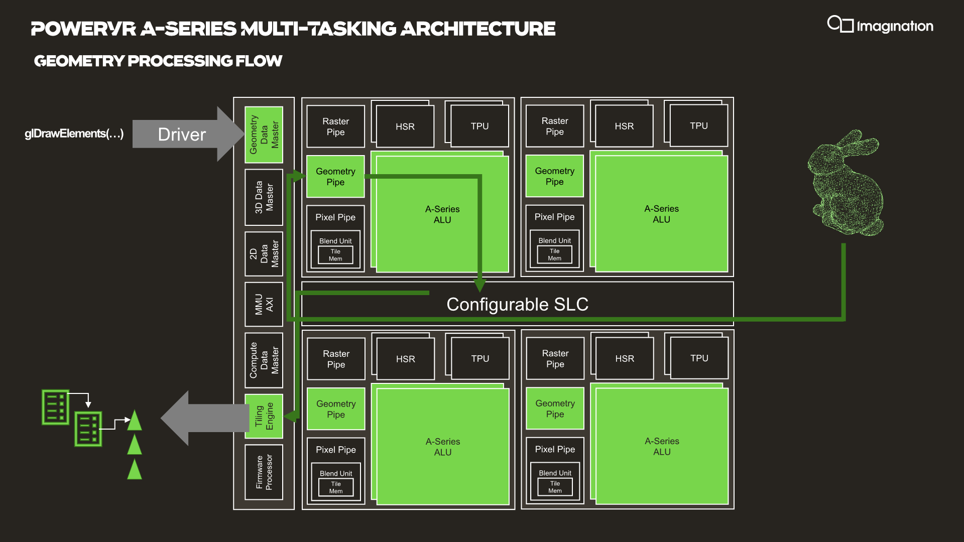
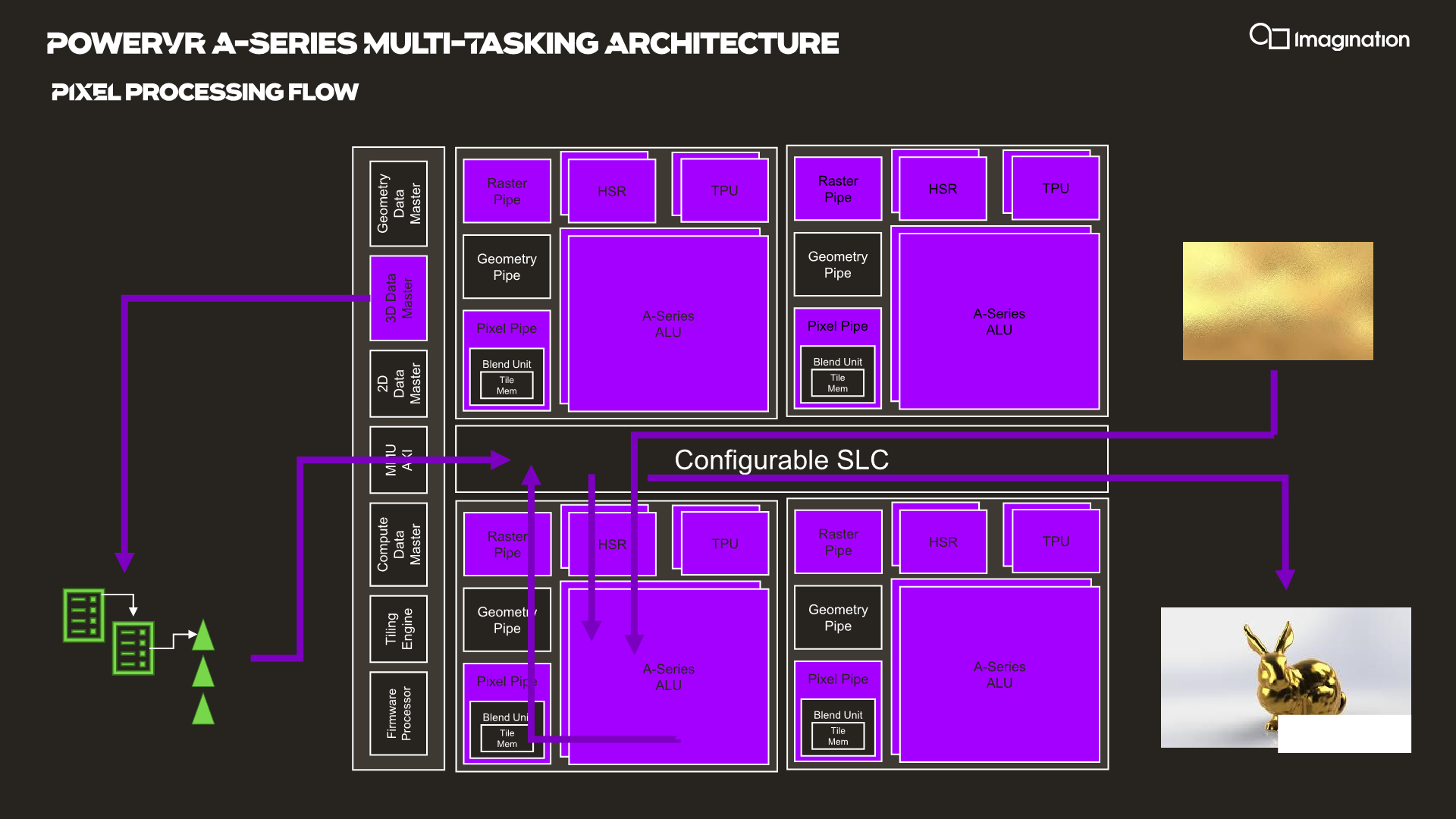
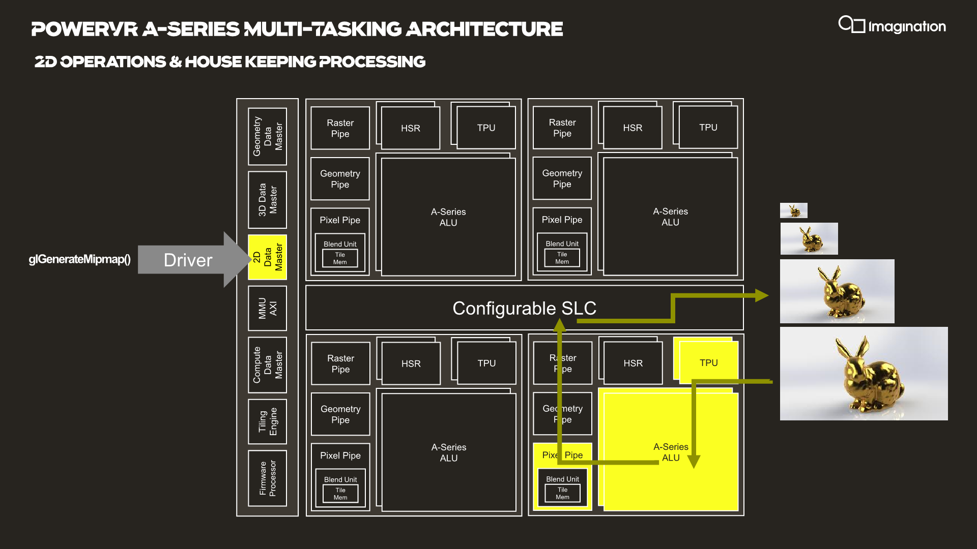
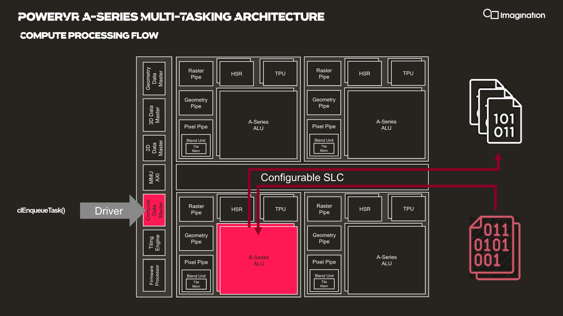
In your usual rendering flows, there are different kinds of “master” controllers each handling the dispatching of workloads to the GPU; geometry is handled by the geometry data master, pixel processing and shading by the 3D data master, 2D operations are handled by the 2D data, master, and compute workloads are processed by the, you guessed it, the compute data master.
In each of these processing flows various blocks of the GPU are active for a given task, while other blocks remain idle.
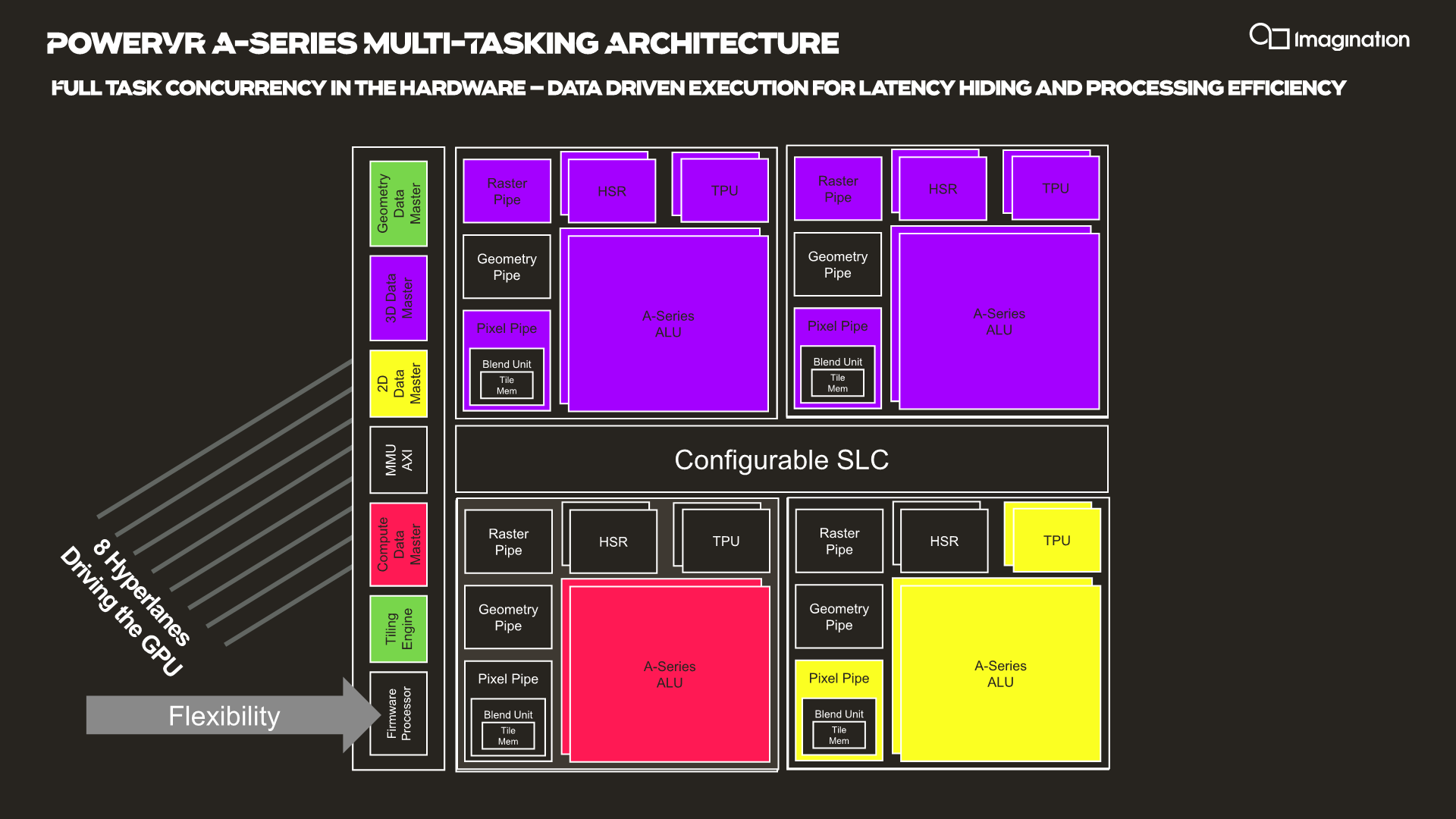
HyperLane technology is said to be able to enable full task concurrency of the GPU hardware, with multiple data masters being able to be active simultaneously, executing work dynamically across the GPU’s hardware resources. In essence, the whole GPU becomes multi-tasking capable, receiving different task submissions from up to 8 sources (hence 8 HyperLanes).
The new feature sounded to me like a hardware based scheduler for task submissions, although when I brought up this description the Imagination spokespeople were rather dismissive of the simplification, saying that HyperLanes go far deeper into the hardware architecture, with for example each HyperLane having being able to be configured with its own virtual memory space (or also sharing arbitrary memory spaces across hyperlanes).
Splitting GPU resources can happens on a block-level concurrently with other tasks, or also be shared in the time-domain with time-slices between HyperLanes. Priority can be given to HyperLanes, such as prioritizing graphics over a possible background AI task using the remaining free resources.
The security advantages of such a technology also seem advanced, with the company use-cases such as isolation for protected content and rights management.
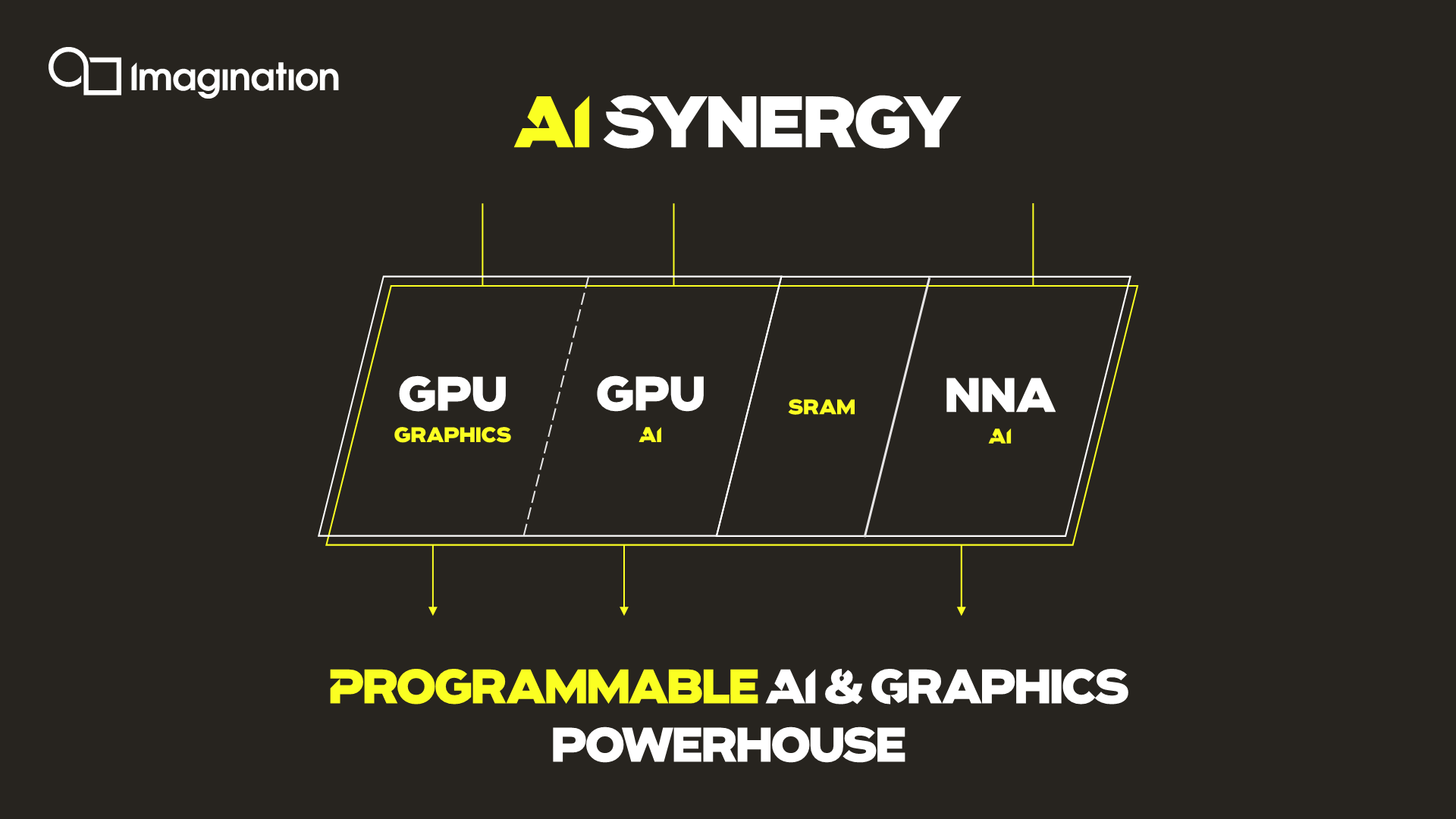
An interesting application of the technology is the synergy it allows between an A-Series GPU and the company’s in-house neural network accelerator IP. It would be able to share AI workloads between the two IP blocks, with the GPU for example handling the more programmable layers of a model while still taking advantage of the NNA’s efficiency for the fixed function fully connected layer processing.
Three Dozen Other Microarchitectural Improvements
The A-Series comes with other numerous microarchitectural advancements that are said to be advantageous to the GPU IP.

One such existing feature is the integration of a small dedicated CPU (which we understand to be RISC-V based) acting as a firmware processor, handling GPU management tasks that in other architectures might be still be handled by drivers on the host system CPU. The firmware processor approach is said to achieve more performant and efficient handling of various housekeeping tasks such as debugging, data logging, GPIO handling and even DVFS algorithms. In contrast as an example, DVFS for Arm Mali GPUs for example is still handled by the kernel GPU driver on the host CPUs.
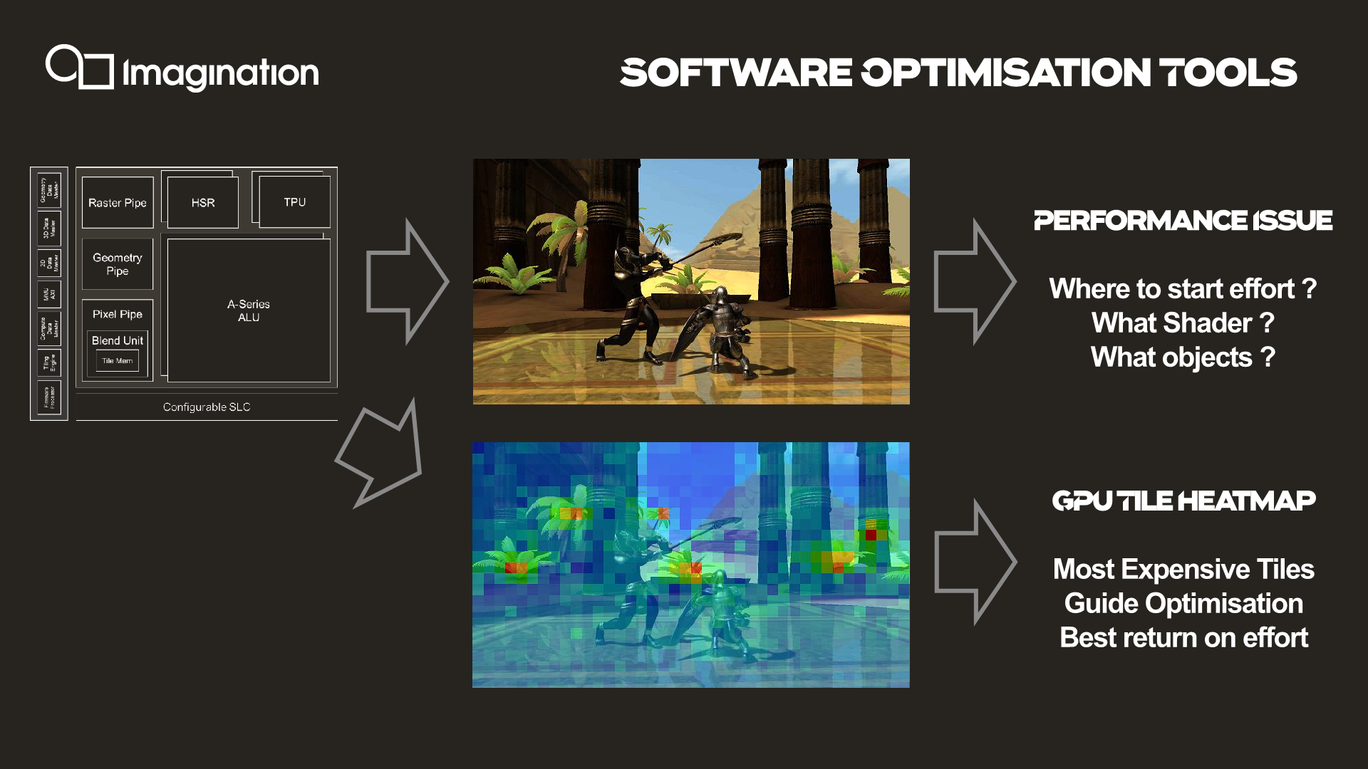
An interesting new development feature that is enabled by profiling the GPU’s hardware counters through the firmware processor is creating tile heatmaps of execution resources used. This seems relatively banal, but isn’t something that’s readily available for software developers and could be extremely useful in terms of quick debugging and optimizations of 3D workloads thanks to a more visual approach.


143 Comments
View All Comments
mode_13h - Monday, December 9, 2019 - link
Nah, not in GPU parlance. Nvidia has long talked about each element of a SIMD as a thread. What CPU folks would call a "thread", Nvidia calls a "warp" and AMD calls a "wave". Not sure what Imagination calls it.ballsystemlord - Friday, December 20, 2019 - link
Grammar error:"...with for example each HyperLane having being able to be configured with its own virtual memory space..."
Excess words, try:
"...with for example each HyperLane having to be configured with its own virtual memory space..."
Fataliity - Saturday, December 28, 2019 - link
I bet you this GPU IS the Intel one, and Furian is the Ice Lake one. 64EU's at 1TFLOP = Ice Lake, 1GHz. Furian is 1/2 the speed of the A series.Intel's GPU is Xe. thisi s A - XE, XT, XM
But the base of 1/16 is called..... XE.
Add to that this
https://news.synopsys.com/2016-03-31-Intel-Custom-...
"certified on Intel 10nm PowerVR GT7200"
Who's buying this on Intel's process, and why is it ceritifed on IMGtech's GPU, if its not their integrated graphics under a different name?