Intel’s 2021 Exascale Vision in Aurora: Two Sapphire Rapids CPUs with Six Ponte Vecchio GPUs
by Dr. Ian Cutress on November 17, 2019 7:01 PM EST- Posted in
- CPUs
- Intel
- HPC
- Enterprise
- GPUs
- Aurora
- Exascale
- Xe
- Sapphire Rapids
- Ponte Vecchio
For the last few years, when discussing high performance computing, the word 'exascale' has gone hand-in-hand with the next generation of supercomputers. Even last month, on 10/18, HPC twitter was awash with mentions of ‘Exascale Day’, signifying 10^18 operations per second (that’s 10 million million million). The ‘Drive to Exascale’ is one of the key targets in the next decade for the supercomputing market, and Intel is going in with the Aurora Supercomputer ordered by the Argonne National Laboratory.
Intel has been working on the Aurora contract for a while now, and the project has changed scope over time due to market changes and hardware setbacks. Initially announced several years ago as a ‘deliver by 2020’ project between Argonne, Cray, and Intel, the hardware was set to be built around Intel’s Xeon Phi platform, providing high-throughput acceleration though Intel's AVX-512 instructions and the 10nm Knights Hill accelerator. This announcement was made before the recent revolution in AI acceleration, as well as Intel subsequently killing off the Xeon Phi platform after adding AVX-512 to its server processors (with the last breath Knights Mill receiving a very brief lifespan). Intel had to go back to the drawing board, and since Xeon Phi was scrapped, Intel’s audience has been questioning what it will bring to Aurora, and until today the company had only said that it would be built from a combination of Xeon CPUs and Xe GPUs.
An Aurora Node
As part of today’s announcement, Intel has put some information on the table for a typical ‘Aurora’ compute note. While not giving any specifics such as core counts or memory types, the company stated that a standard node will contain two next generation CPUs and six next generation GPUs, all connected via new connectivity standards.
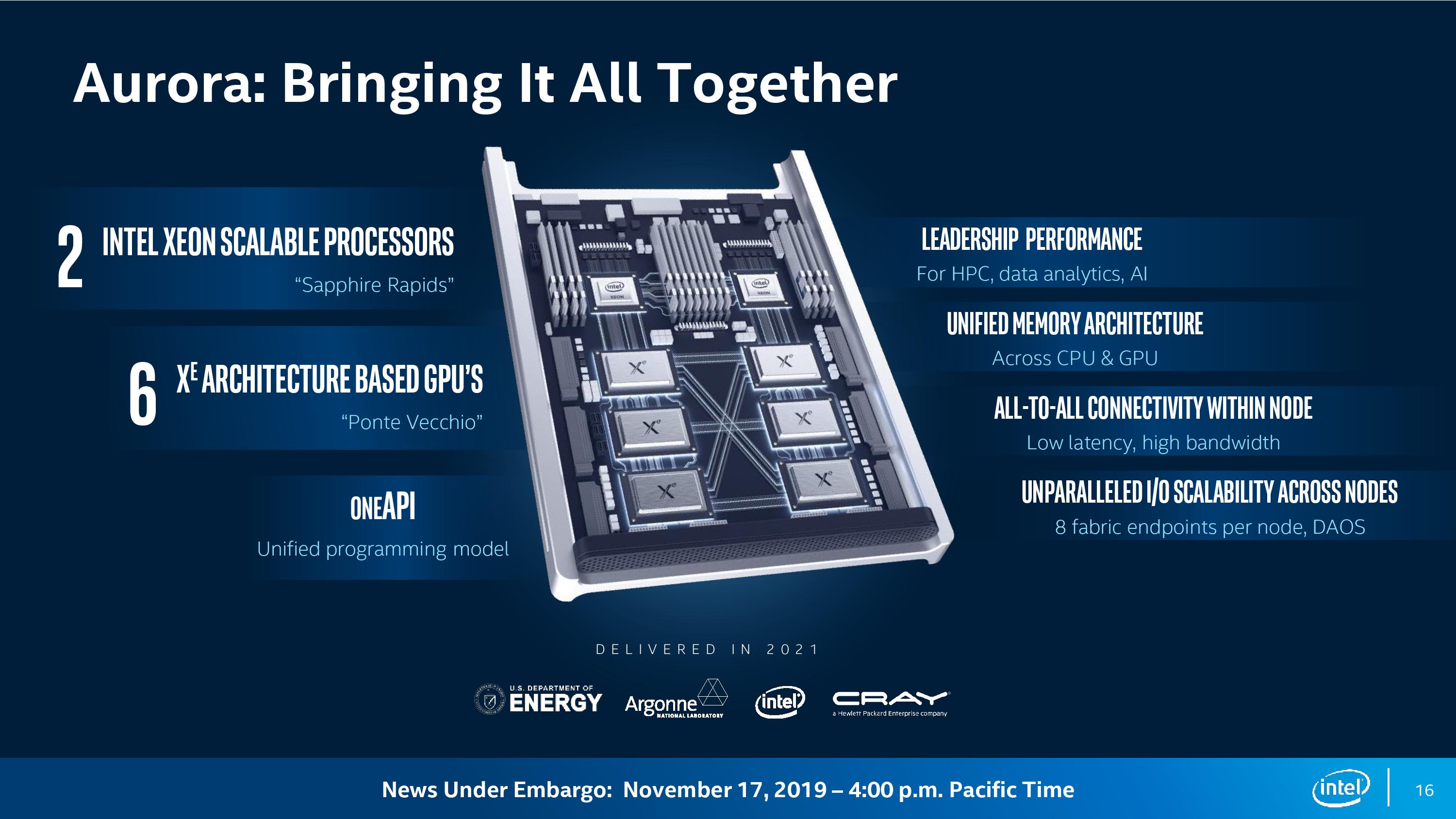
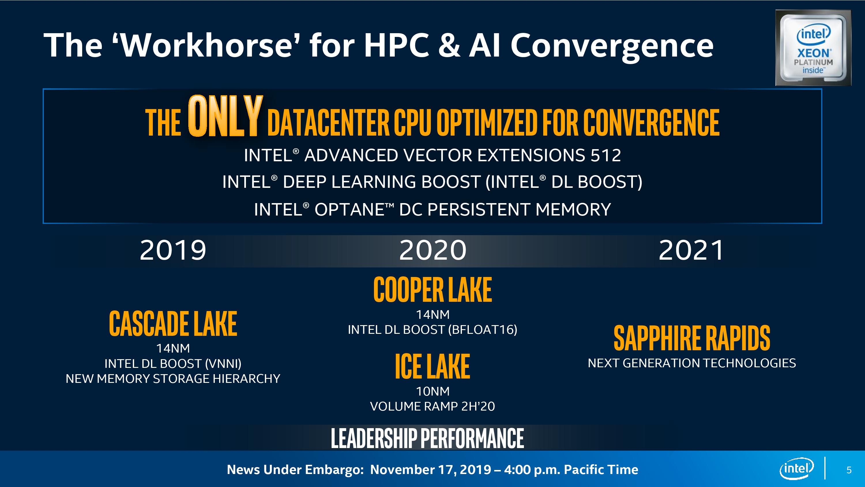
Those CPUs will be Sapphire Rapids CPUs, Intel’s second generation of 10nm server processors coming after the Ice Lake Xeons. The announcement today reaffirmed that Sapphire Rapids is a 2021 processor; and likely a late 2021 processor, as the company also confirmed that Ice Lake will have its volume ramp through late 2020. Judging from Intel's images, Sapphire Rapids is set to have eight memory channels per processor, with enough I/O to connect to three GPUs. Within an Aurora node, two of these Sapphire Rapids CPUs will be paired together, and support the next generation of Intel Optane DC Persistent Memory (2nd Gen Optane DCPMM). We already know from other sources that Sapphire Rapids is likely to be DDR5 as well, although I don't believe Intel has said that outright at this point.
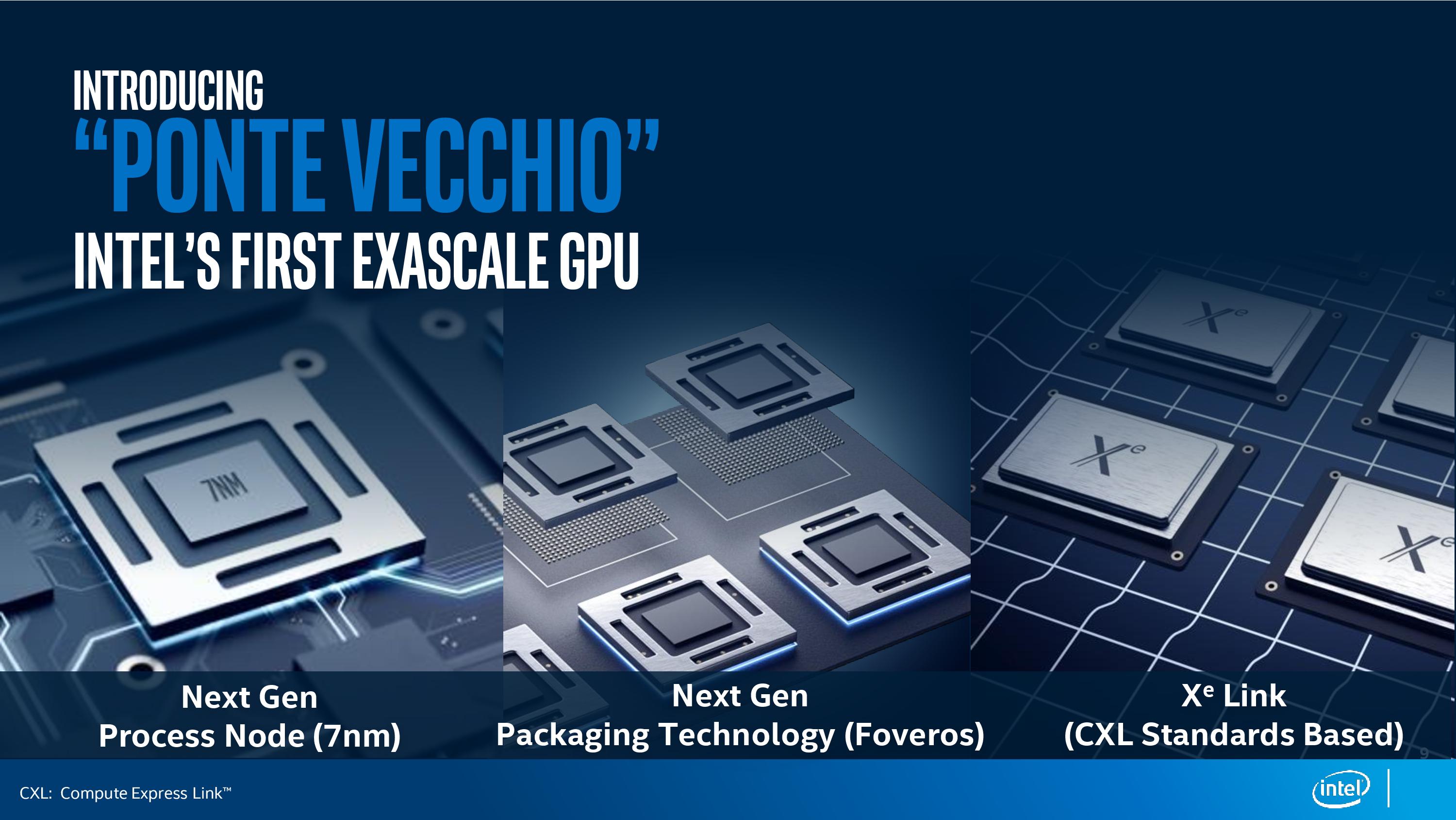
On the GPU side, all six of the GPUs per node will be Intel’s new 7nm Ponte Vecchio Xe GPU. As we covered in the Ponte Vecchio (PV) announcement, the basis of PV will be in small 7nm chiplets built on a microarchitecture variant of the Xe architecture. PV will employ a key number of Intel’s packaging technologies, such as Foveros (die stacking), Intel’s Embedded Multi-Die Interconnect Bridge (EMIB), and high bandwidth cache and memory. With regards to capabilities, Intel has only stated that PV will have a vector matrix unit and high double precision performance, which is likely going to be required for the research that Argonne performs.
The other core technology in an Aurora node is the use of the new Compute eXpress Link (CXL) standard. CXL will allow the CPUs and GPUs to connect directly together and work within a unified memory space. Intel stated in our briefings that the GPUs will be connected in an all-to-all topology, even though the imagery they provided doesn’t show that. In the diagram it shows every PV GPU connected to three others, with the top GPUs connected directly to the CPU. It is unclear if the CPUs talk to each other through CXL at this point, and what parts of the CXL standard Aurora will be using, however as CXL is based on the PCIe 5.0 physical standard, it will be interesting to see how (or if) Intel produces hardware for each interconnect standard.
Each Aurora node will have 8 fabric endpoints, giving plenty of topology connectivity options. And with the system being built in part by Cray, connecting the systems will be a version of their Slingshot networking architecture, which is also being used for the other early-2020s US supercomputers. Intel has stated that Slingshot will connect ~200 racks for Aurora, featuring a total of 10 petabytes of Memory and 230 petabytes of Storage.
Guessing Ponte Vecchio Performance
With this information, if we spitball some numbers on performance, here's what we end up with:
- Going with Intel's number of 200 racks
- Assume each rack is a standard 42U,
- Each Aurora node is a standard 2U,
- We know the system has 200 racks.
- Take out 6U per rack for networking and support,
- Take out 1/3 of the racks for storage and other systems
- We get a rounded value of 2400 total Aurora nodes (2394 based on assumptions).
This means we get just south of 5000 Sapphire Rapids CPUs and 15000 Ponte Vecchio GPUs for the whole of Aurora. Now when calculating the total performance of a supercomputer, the CPU and Accelerator performance often depends on the workload required. If Ponte Vecchio is truly an exascale class GPU, then let’s assume that the GPUs are where the compute is. If we divide 1 ExaFLOPs by 15000 units, we’re looking at 66.6 TeraFLOPs per GPU. Current GPUs will do in the region of 14 TF on FP32, so we could assume that Intel is looking at a ~5x increase in per-GPU performance by 2021/2022 for HPC. Of course, this says nothing about power consumption, and if we were to do the same math at 4U per node, then it would be ~7500 GPUs, and we would need 135 TF per GPU to reach exascale.
Delivering The Hardware
Despite initially being a ‘deliver by 2020’ project, Intel is now saying that Aurora will be delivered in 2021. This means that Intel has to execute on the following:
- Manufacturing at 10++ in sufficient yield with respect to cores/frequencies
- Manufacturing at 7nm for chiplets, both in yield and frequencies
- Transition through DDR3 to DDR4 (and DDR5?) in that time frame
- Transition through PCIe 3.0 to PCIe 4.0 and PCIe 5.0 in that time frame
- Release and detail its 2nd generation Optane DC Persistent Memory
- Provide an SDK to deal with all of the above
- Teach researchers to use it
On those last two points, Intel has stated that Ponte Vecchio and Aurora will be a primary beneficiary of the company’s new OneAPI SDK. This industry initiative, spearheaded by Intel, is designed to use a singular cross-architecture language called ‘Data Parallel C++’, based on C++ and SYCL, that can pull libraries designed to speak to various elements of Intel’s hardware chain. The idea is that software designs can write the code once, link appropriate libraries, and then cross-compile for different Intel hardware targets. In Intel’s parlance, this is the ‘xPU’ strategy, covering CPU, GPU, FPGA, and other accelerators. Aside from Argonne/Cray, Intel is citing Lenovo and Atos as key partners in the OneAPI strategy.

In order to achieve a single exascale machine, you need several things. First is hardware – the higher performance a single unit of hardware, the fewer you need and the less infrastructure you need. Second is infrastructure, and being able to support such a large machine. Third is the right problem that doesn’t fall afoul of Amdahl’s Law – something that is so embarrassingly parallel that can be spread across all the hardware in the system is a HPC scientist dream. Finally, you need money. Buckets of it.
In the past few years, the top supercomputers in the world have addressed all of these requirements by orders of magnitude: hardware is faster, infrastructure is readily available, traditionally serial problems are being re-architected to be parallel (or lower precision), and governments are spending more than ever for single supercomputers. A $5 million supercomputer used to get a research group into the top echelons of the Top 500 list. Now it’s more like $150+ million. The current leader, Summit, had an estimated build cost of $200 million. And Aurora will handily top that, with the deal valued at more than $500 million.
When I asked before the announcement if Argonne would be the first customer of Ponte Vecchio, the Intel executive heading the briefing dodged the question by instead answering his own, saying ‘we’re not disclosing other customers’. In all my time as a journalist, I don’t think I’ve ever had a question unanswered and dodged in such a way. Unfortunately I had no opportunity in the open Q&A session to follow up.
Ultimately, based on what we know so far, Intel still has a lot of work to do to deliver this by 2021. It may be the case that Aurora is that culmination of all its technologies, and that Intel would be prepared to use the opportunity to help smooth out any issues that might arise. At any rate, some of these technologies might not get in the hands of the rest of us until 2022.
Hopefully, when Aurora is up and running, we’ll get a chance to take a look. Watch this space.
Related Reading
- Intel's Interconnected Future: Combining Chiplets, EMIB, and Foveros
- Intel to Support Hardware Ray Tracing Acceleration on Data Center Xe GPUs
- Intel’s Xeon & Xe Compute Accelerators to Power Aurora Exascale Supercomputer
- Intel Details Manufacturing through 2023: 7nm, 7+, 7++, with Next Gen Packaging


43 Comments
View All Comments
outsideloop - Sunday, November 17, 2019 - link
"Leadership Performance" I love good comedic content.IntelUser2000 - Monday, November 18, 2019 - link
"Third" Gen Optane DIMM, not Second.By the way if you assume the whole setup is 40MW, and you further assume the 2400 nodes use 90% of the power, you end up with a single node consisting of 2x Sapphire Rapids and 6x Ponte Vecchio using 15KW. So maybe 80% of that is the GPU, so each Ponte Vecchio is using 2KW.
IntelUser2000 - Monday, November 18, 2019 - link
Based on that the improvement over the current GPU is 10x, because supercomputers care about FP64 not FP32. 6.7x more power for 10x more performance equals 50% more efficiency. That makes more sense.MrSpadge - Monday, November 18, 2019 - link
Or maybe your assumption of 40 MW is wrong?Santoval - Monday, November 18, 2019 - link
I strongly doubt a single Ponte Vecchio will draw 2 kW. Even my boiler does not require 2 kW. As for the assumed 15 kW for a single 2U node I am pretty sure such a power density would rival that of nuclear reactor cores.Yojimbo - Monday, November 18, 2019 - link
In terms of HPC, exascale means FP64 performance, not FP32 performance.The Summit supercomputer has over 27,000 Tesla V100s and uses about 13 MW. The Aurora Supercomputer will be a ~30 MW machine. My guess is either there will be 50,000+ GPUs or their GPUs are going to be made very large using the chiplet technology.
IntelUser2000 - Monday, November 18, 2019 - link
Yes it looks like we're going from 300W GPUs that look like a video card, to a much larger one using 1-2KW but with much more performance. Intel's presentation about the card using 8 MCM GPU die is evidence of that.Yojimbo - Monday, November 18, 2019 - link
Many of the NVIDIA HPC GPUs already don't look like a video card, they use a mezzanine connection. Making the GPUs draw so much power (more than 1 kW) creates a rather specialized solution because I am not sure hyperscalers and cloud builders are set up to cool and power such beasts. Of course, with the chiplet approach it will be less work to scale it down to something more manageable, but I don't think Intel has that concern in mind with their first generation of compute GPUs; they can't expect much commercial uptake, anyway. I would think they would want some sort of lower power developer boards available, however, to start to go after the commercial market.Kevin G - Monday, November 18, 2019 - link
This reads like an architecture that Intel wants to win the performance crown. At a high level, the technology is there with the potential to do it as they are throwing a lot of silicon at the problem.I am not surprised about the large power budget and it is something I've expected once the move to chiplets begin. There are three effective caps on power consumption: chip size, voltage and frequency. One of the caps has been removed and thus a spike in how much energy can be put toward a product. Thermo dynamics still reigns supreme but all that heat being generated is spread out over a larger area, something not possible with monolithic designs.
The good news with a chiplet designs is that creating a low power developer board just means scaling back the amount of chiplets. I'd imagine it'd be two compute dies, a Rambo cache die and some HBM would easily fit into a PCIe card's power budget.
Yojimbo - Monday, November 18, 2019 - link
Oh, a minor correction. The original Aurora machine built around the Knights Hill Xeon Phi was supposed to be delivered in 2018, not 2020.