EUV Demand is Up: EUV Device Manufacturer ASML Beats Sales Estimates
by Anton Shilov on October 16, 2019 6:15 PM EST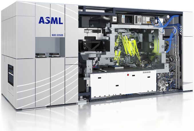
Between the smartphone revolution, cloud computing, and the Internet of Things, the demand for cutting-edge chips has never been higher. And if you have any doubts about that, then one only needs to look at the record-breaking sales of the equipment used to fab those chips. ASML, the leader in the field for photolithography, announced this week its financial results for the third quarter, revealing that its sales, profits, and net bookings all topped expectations, as the company received orders for 23 extreme ultraviolet lithography (EUVL) tools.
ASML’s revenues in Q3 2019 totaled €2.987 billion ($3.3 billion), with a net income of €627 million ($692.7 million). During the quarter, ASML sold 45 DUV and seven EUV lithography systems, as well as five used lithography systems. In total, the company sold 136 step-and-scan tools this year so far, of which 18 were EUV tools. In Q4, the company intends to ship eight EUV step-and-scan systems, bringing the total for 2019 to 30 EUV systems.
ASML’s biggest bump in the third quarter came from a total of 23 orders for Twinscan NXE EUV systems from various customers. Combined with other bookings, ASML’s net bookings totaled €5.111 billion in Q3, the company’s highest ever for a single quarter. It is particularly noteworthy that ASML reaffirmed that it expects its EUV tools to be adopted by both logic makers (i.e., CPUs, GPUs, etc.) and memory manufacturers.
As of July 2018, there were 31 EUV scanners installed at various fabs across the world, including several machines in various semiconductor research organizations. With 10 systems sold in H2 2018 and 18 EUV scanners installed this year, the number of EUV lithography tools used in the world is approaching 60 units. Of course, the number is considerably behind the number of DUV step-and-scan systems used nowadays, but it is clear that extreme ultraviolet lithography is gradually getting more widespread, and that demand is continuing to increase.
Officially, only TSMC and Samsung Foundry use ASML’s Twinscan NXE scanners to make chips using their N7+ and 7LPP manufacturing technologies. Both contract makers of semiconductors will expand their usage of EUV tools as they adopt new fabrication processes. Furthermore, Intel will use EUVL for its 7 nm technology that will be deployed across multiple fabs through 2021. Furthermore, companies like Samsung and SK Hynix are mulling the use of EUVL for DRAM production.
Here is what Peter Wennink, CEO of ASML, had to say:
“For the remainder of the year, we expect Logic to continue to be strong, driven by the leading-edge nodes supporting end-market technology and applications such as 5G and artificial intelligence. The timing of Memory recovery remains uncertain. We continue to make solid progress in EUV. Customers have introduced their first EUV manufactured devices and we have seen EUV mentioned in product announcements. In the third quarter, we shipped seven EUV systems, three of which were NXE:3400C, our higher productivity model. We received 23 EUV orders in the third quarter which contributes to our highest ever value of bookings in one quarter. This strong order flow confirms the adoption of EUV in high volume manufacturing for Logic and Memory. Our overall view for 2019 is essentially unchanged as we continue to see 2019 as a growth year.”
Related Reading:
- ASML to Ship 30 EUV Scanners in 2019: Faster EUV Tools Coming
- Samsung’s Aggressive EUV Plans: 6nm Production in H2, 5nm & 4nm On Track
- TSMC: 3nm EUV Development Progress Going Well, Early Customers Engaged
- Micron’s DRAM Update: More Capacity, Four More 10nm-Class Nodes, EUV, 64 GB DIMMs
- Samsung Completes Development of 5nm EUV Process Technology
Source: ASML


46 Comments
View All Comments
vladx - Thursday, October 17, 2019 - link
Completely irrelevant, I was talking about Philips in the '90s when they gave up ASMLDiogene7 - Thursday, October 17, 2019 - link
To finally have EUV entering High Volume Manufacturing (HVM) is a key milestone, but the usage of EUV will become really significant from the node TSMC 5nm / Samsung 5nm with 10s of layers using EUV and that should start HVM in H1 2020.I am really looking forward to H2 2020 to get my hands on the first devices manufactured with chip manufactured with extensive usage of EUV (Apple iPhone 12 with Apple A14 chip ?).
I consider the 5nm EUV node as really key milestone in humanity history as it will bring chip with 10s of billion of transistor with more than 100 million transistor per mm2.
According to Wikipedia, the first Pentium 4-branded processor to implement 64-bit was the Prescott (90 nm) (February 2004), and it seems it had ~125 millions transistors with a die size of 112mm2.
So in 2020 / 2021, thanks to lithography scaling, with 5nm EUV node, it will be possible to shrink an Intel Pentium 4 Prescott (90nm) processing power in less than 1mm2, while consuming much less energy !!! Amazing !!!
I am wondering if lithography scaling of silicon CMOS will be able to reach the next milestone of 1 billion transistor by 1mm2 : As of 2019, my guess would be that lithography scaling alone of silicon CMOS won’t allow to achieve it, and that there will be a need for new packaging (going 3D with 3D IC), and also new materials (Carbon nanotubes, spintronics,...) to achieve the equivalent of 1 billion transitors per mm2 (not necessarily silicon transistors)
Eliadbu - Thursday, October 17, 2019 - link
We are reaching the limit of how small we can manufacture semiconductors chips and makes them work due various reasons. Density was and still is important aspect (see Moore law which had more impact in different than just mere observation) but as we reach the limit we need to find new methods to increase "compute power" either be 3d stacking to get more transistor in unit of volume or other ways like optical compute.abufrejoval - Friday, October 18, 2019 - link
To label a process node "a keystone of humanity" could be considered a slight exaggeration.ksec - Thursday, October 17, 2019 - link
Thanks Anton, because of you Anandtech is finally covering more industry business news and supply chain partners that dont normally get much attention from consumers.One of the reason I have been sceptical of Intel's EUV claims is based on the ASML numbers, their EUV shipment numbers and forecast does not bold well for Intel. All the current shipment are gong to TSMC and Samsung. Next year will be the same and leaving Intel with very little stocks, which means Intel's 2021 7nm wont have volume anywhere close to TSMC or Samsung.
Anymoore - Monday, October 21, 2019 - link
There are 45 NXE:3400B total to be installed. Only 36 of these will be up on any day, across the world. That's not a lot, compared to the immersion baseline.