Hot Chips 31 Live Blogs: Intel Lakefield and Foveros
by Dr. Ian Cutress on August 20, 2019 7:10 PM EST
07:14PM EDT - One of the interesting developments in packaging technology in recent memory is the 3D stacking of Intel's new Foveros technology. The first chip to use this packaging technology is called Foveros, and today we have a talk on the chip.
07:15PM EDT - Going to start in a minute or so
07:17PM EDT - We know a lot about Lakefield and Foveros: stacked logic and IO die, with POP DRAM. Hybrid x86 with 1x Sunny Cove and 4x Tremont
07:17PM EDT - This is the packaging session on Hot Chips, so we might learn more about the Foveros
07:17PM EDT - Lakefield for smartphone and laptops
07:18PM EDT - Best in class compute in smaller form factor
07:18PM EDT - Customer request
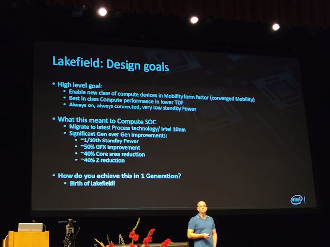
07:18PM EDT - Lots of requirements, including 10nm and 2mW standby Power
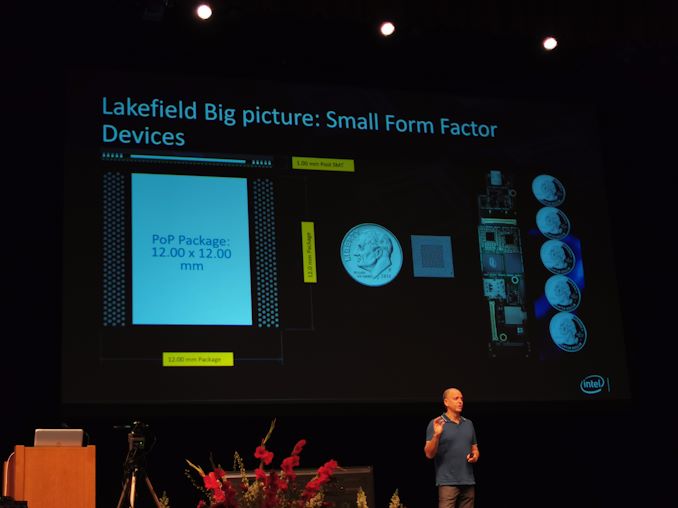
07:19PM EDT - Also had to be small
07:19PM EDT - and high performance
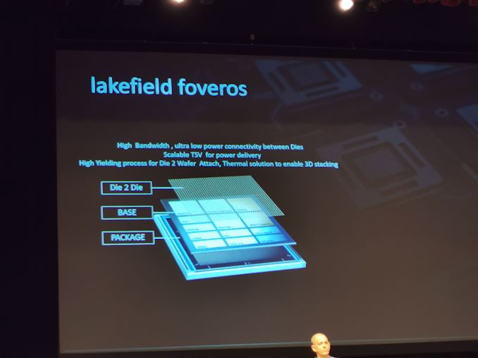
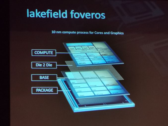
07:20PM EDT - Compute Die, base die, and 4GB (4 Gb?) memory on top
07:20PM EDT - 1mm z-height with post-SMT
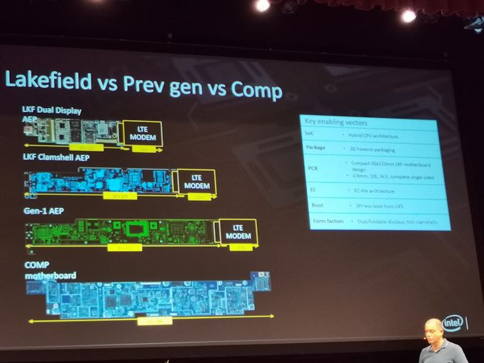
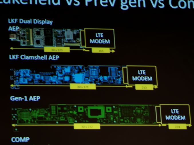
07:21PM EDT - 30x123 PCB for full compute on a PCB
07:21PM EDT - SMallest ever Intel complete solution
07:22PM EDT - Competitor PCB is 43x286 mm
07:22PM EDT - Competitor has onboard LTE modem, Intel does not
07:22PM EDT - LKF Clamshell AEP is what we'll see in notebooks
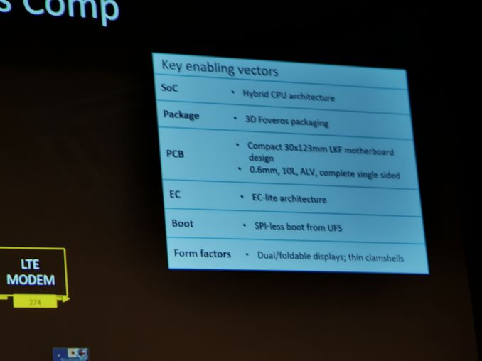
07:22PM EDT - PCB is 10 layer
07:23PM EDT - SPI-less boot from UFS
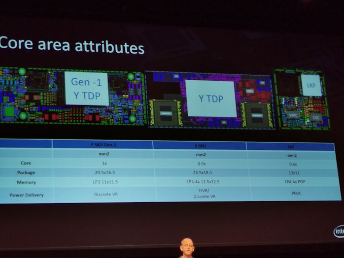
07:23PM EDT - Comparing last gen Y CPU vs LKF
07:24PM EDT - Amber vs Ice-Y vs Lakefield
07:24PM EDT - Power Delivery is PMIC
07:24PM EDT - Two PMICs in LKF, one for Compute die, one for IO die
07:25PM EDT - Compute in 10+
07:25PM EDT - (Once Again, the computer with the demonstration doesn't have the Intel font)
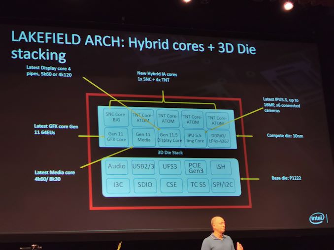
07:25PM EDT - 1x Sunny Cove + 4x Tremont
07:26PM EDT - Can support up to 6 cameras
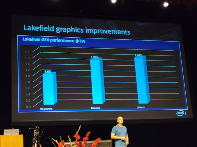
07:26PM EDT - Gen 11 graphics, 64 EUs
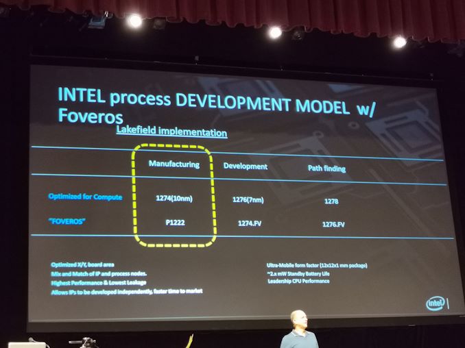
07:26PM EDT - Base Die is P1222
07:28PM EDT - P1222 is 10nm
07:28PM EDT - 7nm in development
07:28PM EDT - Sorry, P1222 isn't 10nm. it's 14nm
07:28PM EDT - Multi-die behaving like a monolithic die
07:29PM EDT - Allows IPs to be developed independently, faster time to market
07:29PM EDT - Plan to make many more stacked SoCs
07:30PM EDT - (This new slide doesn't even have a capital L for Lakefield)
07:31PM EDT - 4 GB DRAM, or 8 GB LPDDR4X solution
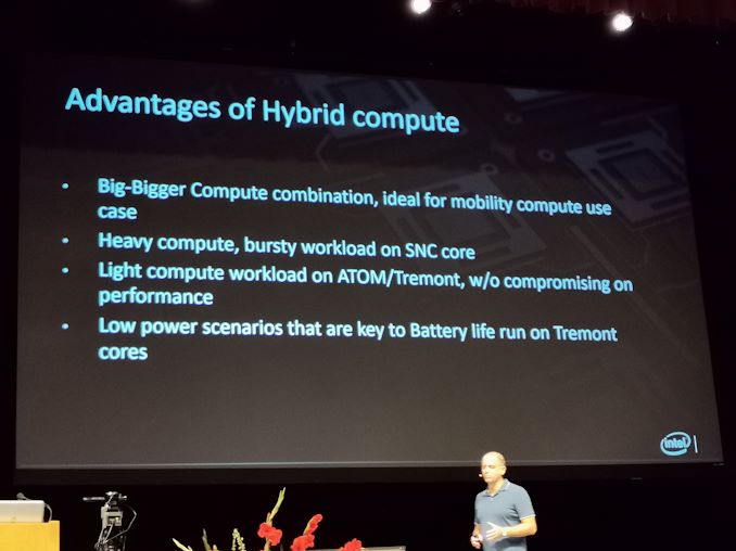
07:31PM EDT - Now hybrid Compute
07:32PM EDT - Low power scenarios key to battery life run on Tremont
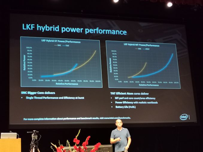
07:32PM EDT - There are power/perf curves for Sunny vs Tremont
07:33PM EDT - ST perf on SNC, low power on Tremont
07:34PM EDT - This slides also say it's better to run MT on Tremont
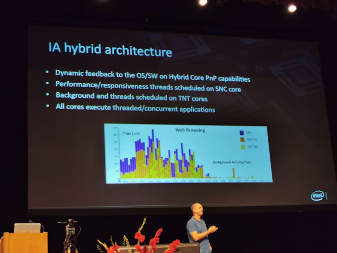
07:34PM EDT - So Sunny is only used for response-type latency workloads
07:34PM EDT - (What this means for multiple workloads running at the same time)
07:35PM EDT - (The person who made these slides really doesn't like capital letters in titles)
07:35PM EDT - Hybrid Architecture shows TNT as base, with SNC being run in specific sections
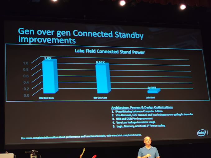
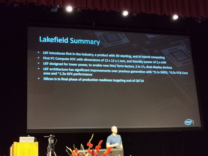
07:36PM EDT - Standby power is 0.08x over Skylake
07:37PM EDT - Vnn removal, LDO removal, low leakage power
07:37PM EDT - No need to use high perf transistors here. Can take advantage of low leakage transistors
07:38PM EDT - First PC Compute SoC
07:38PM EDT - First phase of production, targeting readiness in Q4 2019
07:39PM EDT - Q&A?
07:39PM EDT - Q: Is it 10 or 10+? A: 10+
07:40PM EDT - Q: Interconnect between IO die and Compute die? A: Cut serialization and made it vertical
07:40PM EDT - Q: Face to face bonding of two dies? A: Yes
07:41PM EDT - Q: How is power and IO delivered through that connect? A: Combination of TSVs
07:42PM EDT - Q: pitch of microbumps? A: 50 micron pitch, 20 micron height
07:42PM EDT - Q: Can all the dies function independently or together? A: Can function independently like a normal PC
07:44PM EDT - Q: Penalty for keepaway from vias? A: The design rules are very forgiving - there are many classes of circuits that can be next to vias that can make it work. You won't use high speed, but on this product it was very easy to deliver.
07:45PM EDT - Q: Can you scale to higher power, with like a discrete GPU on top? How does that affect die rules? A: We don't see power limits, we think it will scan the entire range of the spectrum. Or the die to die scaling. It's a question of technology and ramping, then power delivery. It's all about working out the losses. We don't see a big limit from limiting 3D stacking.
07:46PM EDT - Q: Can you stack more dies? Thermals? A: Foveros is CoWoP with Silicon on Silicon, there should be no limit. Benefits of attaching many chiplets. Other pratical limits in architecture partitioning. Our goal is to drive it to many chiplets.
07:46PM EDT - That's a wrap. Now Xeon Jintide!




28 Comments
View All Comments
name99 - Wednesday, August 28, 2019 - link
And 68K to PPC. And reverse ARM to x86 (Project Catalyst).And 32-bit to 64-bit multiple times (PPC, then x86, then ARM).
Most recently (Apple Watch) from 32-bit to 64-bit without even requiring recompilation.
Point is it CAN be done well and efficiently if the company wants it to be done that way.
Of course MS still can't tell, 20+ years after .NET, what its strategy for byte code is... And it took forever to switch to Intel 64-bit.
So, yeah, in the world of MS this may be more of an uphill battle. This is NOT an MS competence.
Wilco1 - Friday, August 23, 2019 - link
The Office apps were not yet native AArch64 according to eg. https://www.windowscentral.com/snapdragon-8cx-benc...Note the 8cx CPU is twice as fast as the fastest Atom, so it can emulate x86 code faster than Atom can run it natively! So if you agree a modern Atom can run Windows well, the 8cx will be fast enough even when emulating.
efferz - Sunday, August 25, 2019 - link
my 8250U gets 7200 marks in Night Raid physics testefferz - Sunday, August 25, 2019 - link
If the 8250U only get 4400 marks,it may run at 2.1GHz.foxmusics - Saturday, August 31, 2019 - link
Well playedhttp://foxmusics.com/download-new-music/
yeeeeman - Wednesday, August 21, 2019 - link
This is a nice development from Intel. Not too afraid that it will give ARM problems, but it is a shame for a big company like Intel not to have some mobile devices in the era of mobile devices. I got it that in 2015 when they had the atom line mobile devices weren't so prevalent, but nowadays they are everywhere and they are starting to become good enough for most use cases. They need this development and they really need to have mobile products. I am pretty confident that they would sell, for the right price and performance.jjj - Wednesday, August 21, 2019 - link
The DRAM amount is highly limiting when even phones are going 16GB.Foldable means high price, if it's a phone it needs integrated modem and if it's high price, it needs more DRAM and more than 1 big core. If it's a tablet, doesn't sell if as large as a phone, if much larger, the display costs stay insane for much longer as yields drop hard with area.
Dual display is just moronic and costly.
This is a solution for low end at best but do they have the costs to target low end?
We'll see if they target something outside consumer but this first gen product doesn't seem to make much sense. If they were using ARM cores, it would have been a different matter, ARM offers so much more in terms of perf density.
HStewart - Thursday, August 22, 2019 - link
I would expect that the 4G on chip is only part of the ran and probably have optional ram outside of chip. Also you got to think of type of device this is, this is not desktop gaming machine and these cores are likely significant faster than ARM cores.name99 - Wednesday, August 28, 2019 - link
"these cores are likely significant faster than ARM cores."Which ARM cores? No way in hell even that SNC core is faster than an A12 Vortex...
A76? Maybe, but A77 maybe not.
As for the 4GB, I think extra DRAM is unlikely. The mechanics become difficult -- two memory controllers and an additional set of DRAM pins?
Go to Best Buy and look. A low end laptop (say $300 and lower) comes with 4GB.
My guess is that this is targeting things that are supposed to be iPad competitors, price maybe $200, crappy 64GB flash, no built in keyboard.
mode_13h - Wednesday, August 21, 2019 - link
So, will the Tremont cores get AVX or not?Maybe the OS will trap the SIGILL and fault AVX threads to the Sunny Cove core. Then, tag them as AVX-users to keep them off the Tremont cores. Still, that would be messed up, if code that's doing runtime checks for CPU instruction support has to keep checking, based on the core it's running on. Or you have a situation where all these threads have affinity for the big core and the Tremonts are just idling away.
So, I'm going to hazard a guess that either Tremont has AVX... or Sunny Cove doesn't.