Hot Chips 31 Analysis: In-Memory Processing by UPMEM
by Dr. Ian Cutress on August 19, 2019 3:15 PM ESTInside the PIM-DRAM and DPU
So as mentioned, each data processing unit (DPU) is put in control of 64 MB of DRAM, leading to 128 DPUs in an 8 GB module. These are built into the DRAM at the same time as manufacturing, but the logic is not as physically dense as regular ASIC logic, making it a high-yielding solution. Ultimately a DRAM die is still mostly DRAM, and the UPMEM states that the DPU size is negligible by comparison. In order to do this, UPMEM created an ASIC-like framework of logic cells, SRAM IPs, and implementation flow. Ultimately the goal was to add these DPUs to an otherwise unmodified DRAM design, and the company states they have succeeded.
The DPU is a 14-stage interleaved pipeline processor, that uses 24 hardware threads to achieve better scaling (apparently only 11 are needed for 100% utilization). On multithreaded code, this creates a 1 instruction/cycle throughput, and the 1 GB/s latency per DPU to its local memory helps hide the threading. There is no operand bypass, and no stall signals.
Each DPU has 88 KB of SRAMs inside, split into 64 KB of WRAM (a data cache equivalent) and 24 KB of IRAM (instruction cache equivalent), with DMA instructions to move data between the DRAM and the WRAM/IRAM. These DMA engine is autonomous, which UPMEM states has little-no-effect on pipeline for performance. There is no actual ‘cache’ here, with the company stating that there are too many threads for actual caches, so instead they rely on the efficient DRAM engine and a tightly coupled bank of SRAM to do that job.

The 14-stage pipeline us a basic in-order threaded CPU with dispatch/fetch/read/format/ALU/merge stages with access to the local SRAMs. The DPU has a 64-bit wide access port to its 64 MB array of main DRAM for loads and stores through an immediate addressing mode, and ultimately control of the DPU is still through the main CPU. No DPU can talk to each other, and the DPUs can only work on their 64 MB of main memory, allowing security separation between the hardware.
The main server CPU has full control over the DPU units through the APIs provided by UPMEM, such that the DPUs can be done on an allocate/free bases or managed through group execution or one-by-one. The DPU doesn’t actually run an OS according to UPMEM, and is controlled just through the device driver.
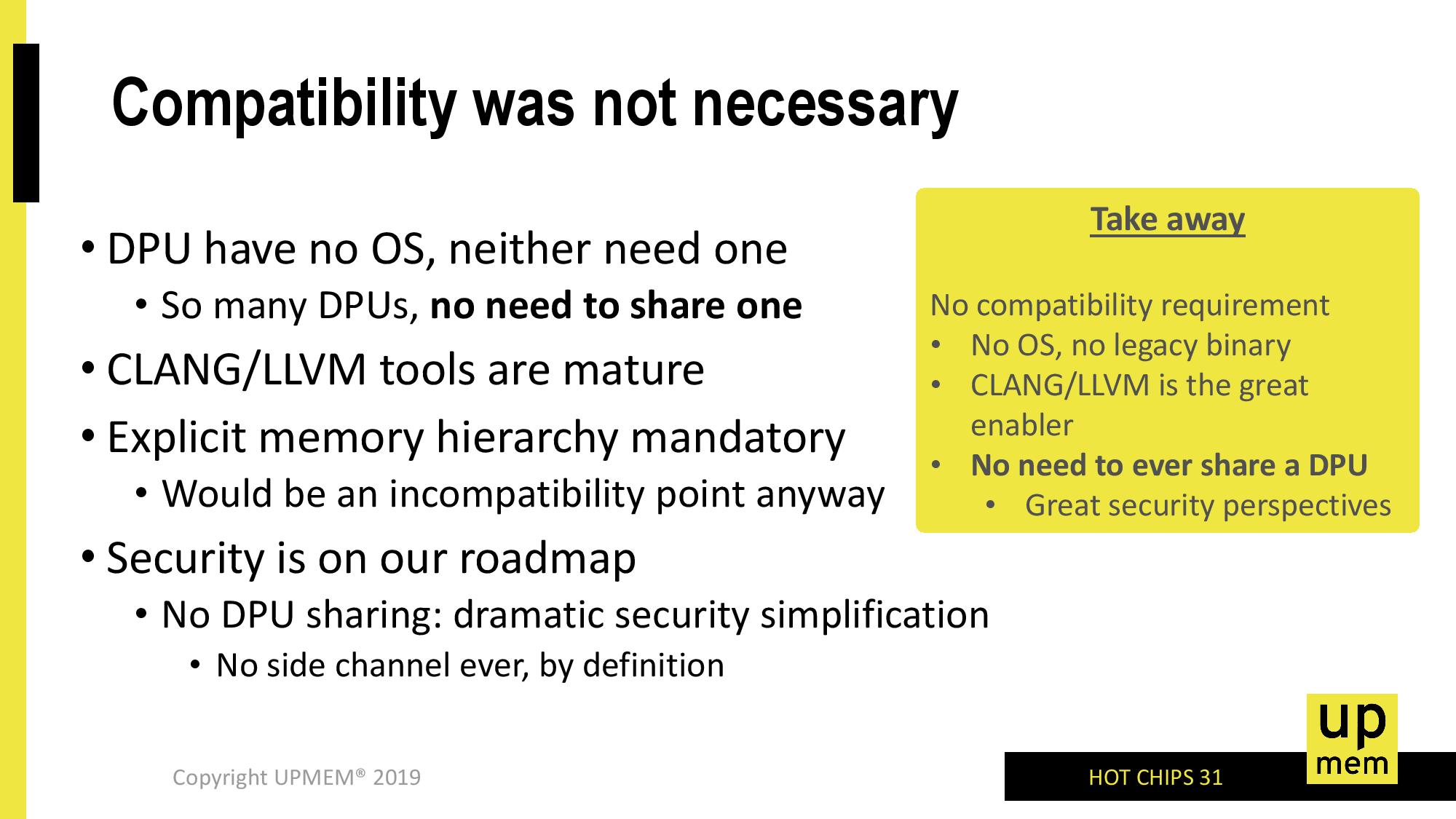
UPMEM states that Clang and LLVM tools are mature to manage DPU use through the compiler and provided APIs. Technically the DPUs have orchestration overhead as a result, and part of this is down to using DDR4 rather than a proprietary interface. UPMEM states that this orchestration management, such as bus width mismatches, address interleaving, the lack of cache coherent and the lack of hardware arbitration, is negligible compared to the work the DPU actually does. The APIs for managing this are available for x86, POWER 9, and ARM64.
Internally the DPU uses an optimized 32-bit ISA with triadic instructions, with non-destructive operand compute. As mentioned, the optimized ISA contains a range of typical instructions that can easily be farmed out to in-memory compute, such as SHIFT+ADD/SHIFT+SUB, basic logic (NAND, NOR, ORN, ANDN, NXOR), shift and rotate instructions, and even compute that requires intermediate values. The DPU supports bi-endianess, and is host OS agnostic.
The Goal
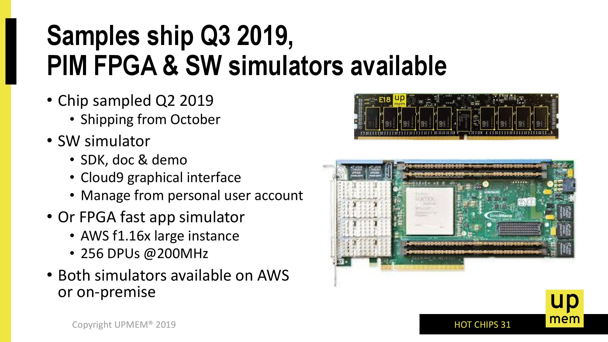
UPMEM is presenting its technology at Hot Chips as an attempt to attract potential customers, and is looking at mass production of its 8 GB memory modules in Q1, although early customers are already being sampled. The company is set to launch a sales office in the Bay Area during the second half of 2019.
The company is putting up impressive numbers for specific workloads, and to be honest, the question of in-memory compute is not really a question of if, but when. Even on the consumer side, there are some good examples where in-memory compute could help. I enjoyed going through UPMEM’s slide decks and looking at what they have to offer. It will be interesting to see other competing solutions come to the market, and how they approach the problem.
I will finish this article on one important note, however. Going up to 20W per 8 GB memory module is not a long-term solution. One of the disadvantages of moving compute away from the CPU is that you have to spend that compute power elsewhere, and a DRAM module isn’t usually the most ideal solution for that based on historic design (especially if doing the calculation is half as efficient). If a CPU socket can hold 150W, and a memory socket can do 20W, then you want most of the power consumed on the compute in the socket. In-memory compute is a good problem to solve, but ultimately it needs to be combined with on-CPU DRAM.


38 Comments
View All Comments
philehidiot - Wednesday, August 21, 2019 - link
Kill joy. But thanks for playing along with my drunken, technically illiterate comments.FunBunny2 - Tuesday, August 20, 2019 - link
"The idea behind In-Memory Processing, or ‘Processing In-Memory’, is that a number of those simple integer or floating point operations should be done while the memory is still in DRAM – no need to cart it over to the CPU, do the operation, and then send it back."FWIW, back in the late 70s TI built a mini, and later a chip with the ISA, which had only a couple of registers. One was an instruction pointer another was the context pointer and perhaps one or two more. All instructions were executed on memory resident data. Deja Vu all over again.
SaberKOG91 - Friday, August 23, 2019 - link
Those were stack machines and were quickly replaced by virtual machines running on RISC processors for efficiency sake. In Flynn's Taxonomy these fall more into the category of MIMD (Multiple Instruction Multiple Data) machines, whereas stack machines are SISD (Single-Instruction Single Data) machines. These chips are basically a modern take on the Stanford VIRAM processors from the late 90's early 00's. Their biggest advantage has to do with not needing to swap RAM in and out of caches to access all of it. If you could bypass the data caches and directly access RAM from the CPU you may incur higher latencies, but the energy cost wouldn't be as bad as you might think.abufrejoval - Tuesday, August 27, 2019 - link
The TMS9900 microprocessor did indeed use a RAM based register file to save CPU transistors while supporting a full 16-bit architecture in those 8-bit days. But that was only possible because even the simplest instructions typically took several clock cycles to complete back then so the overhead of accessing a RAM based register file didn't matter that much if any: Operating on RAM didn't slow computation, truly justifying the Random Access Memory name. Today RAM is the new tape even with 3-4 levels of cache memory.In the case of the TMS9900 data did actually get carried back and forth twice as often, as it as transferred over a multiplexed 8-bit RAM bus to the non-multiplexed 16-bit 256 Byte scratchpad RAM that represented the register file and then would do ALU operations with CPU-RAM read-write operations only to transfer the results back to ordinary RAM afterwards.
TI lost $111 on that venture, perhaps another reason not to repeat that approach.
blacklion - Friday, August 23, 2019 - link
I wonder, how memory allocation is done from point of veiw of Host?They write: work is submitted to DPU via some OS driver. Ok, this part is clear.
But it is only half of the story. DPUs works with physical memory. User-level code (on host processor) works with virtual addresses. So, to prepare task for DPU it needs to know virtual to physical translation, which is typically not allowed for user programs.
And even worse: it needs to allocate chunks of memory in contiguous physical (not virtual!) address space. Again, typical OSes doesn't have such API.
Example: we want to add two arrays of float32 and store result into third. Let say for sake of simplicity, each source array is 16MiB. So, we need to allocate 3 chunks of 16MiB in SAME 64MiB PHYSICAL SPACE to be able to process this data with DPUs! As far as I know, no general-purpose OS supports such allocations!
And it could not be solved with "simple driver", it is changes to very heart of virtual memory subsystem of OS.
I can not find anything about this part in slide deck :(
TomWomack - Thursday, August 29, 2019 - link
That's exactly the same problem as allocating memory on GPU, though at least accessing the memory from the CPU requires only (careful - the CPU cache hierarchy doesn't know about the processors in the memory!) cache invalidation rather than trips over a PCIe bus.ThopTv - Wednesday, August 28, 2019 - link
One of the key critical future elements about this world of compute is moving data about. Moving data requires power, to the point where calling data fromSenbon-Sakura - Thursday, November 18, 2021 - link
As the large bandwidth of DRAM, I guess the vector instructions will achieve more gains for upmem, but why only the scalar instructions are supported in it?