Hot Chips 31 Analysis: In-Memory Processing by UPMEM
by Dr. Ian Cutress on August 19, 2019 3:15 PM ESTInside the PIM-DRAM and DPU
So as mentioned, each data processing unit (DPU) is put in control of 64 MB of DRAM, leading to 128 DPUs in an 8 GB module. These are built into the DRAM at the same time as manufacturing, but the logic is not as physically dense as regular ASIC logic, making it a high-yielding solution. Ultimately a DRAM die is still mostly DRAM, and the UPMEM states that the DPU size is negligible by comparison. In order to do this, UPMEM created an ASIC-like framework of logic cells, SRAM IPs, and implementation flow. Ultimately the goal was to add these DPUs to an otherwise unmodified DRAM design, and the company states they have succeeded.
The DPU is a 14-stage interleaved pipeline processor, that uses 24 hardware threads to achieve better scaling (apparently only 11 are needed for 100% utilization). On multithreaded code, this creates a 1 instruction/cycle throughput, and the 1 GB/s latency per DPU to its local memory helps hide the threading. There is no operand bypass, and no stall signals.
Each DPU has 88 KB of SRAMs inside, split into 64 KB of WRAM (a data cache equivalent) and 24 KB of IRAM (instruction cache equivalent), with DMA instructions to move data between the DRAM and the WRAM/IRAM. These DMA engine is autonomous, which UPMEM states has little-no-effect on pipeline for performance. There is no actual ‘cache’ here, with the company stating that there are too many threads for actual caches, so instead they rely on the efficient DRAM engine and a tightly coupled bank of SRAM to do that job.

The 14-stage pipeline us a basic in-order threaded CPU with dispatch/fetch/read/format/ALU/merge stages with access to the local SRAMs. The DPU has a 64-bit wide access port to its 64 MB array of main DRAM for loads and stores through an immediate addressing mode, and ultimately control of the DPU is still through the main CPU. No DPU can talk to each other, and the DPUs can only work on their 64 MB of main memory, allowing security separation between the hardware.
The main server CPU has full control over the DPU units through the APIs provided by UPMEM, such that the DPUs can be done on an allocate/free bases or managed through group execution or one-by-one. The DPU doesn’t actually run an OS according to UPMEM, and is controlled just through the device driver.
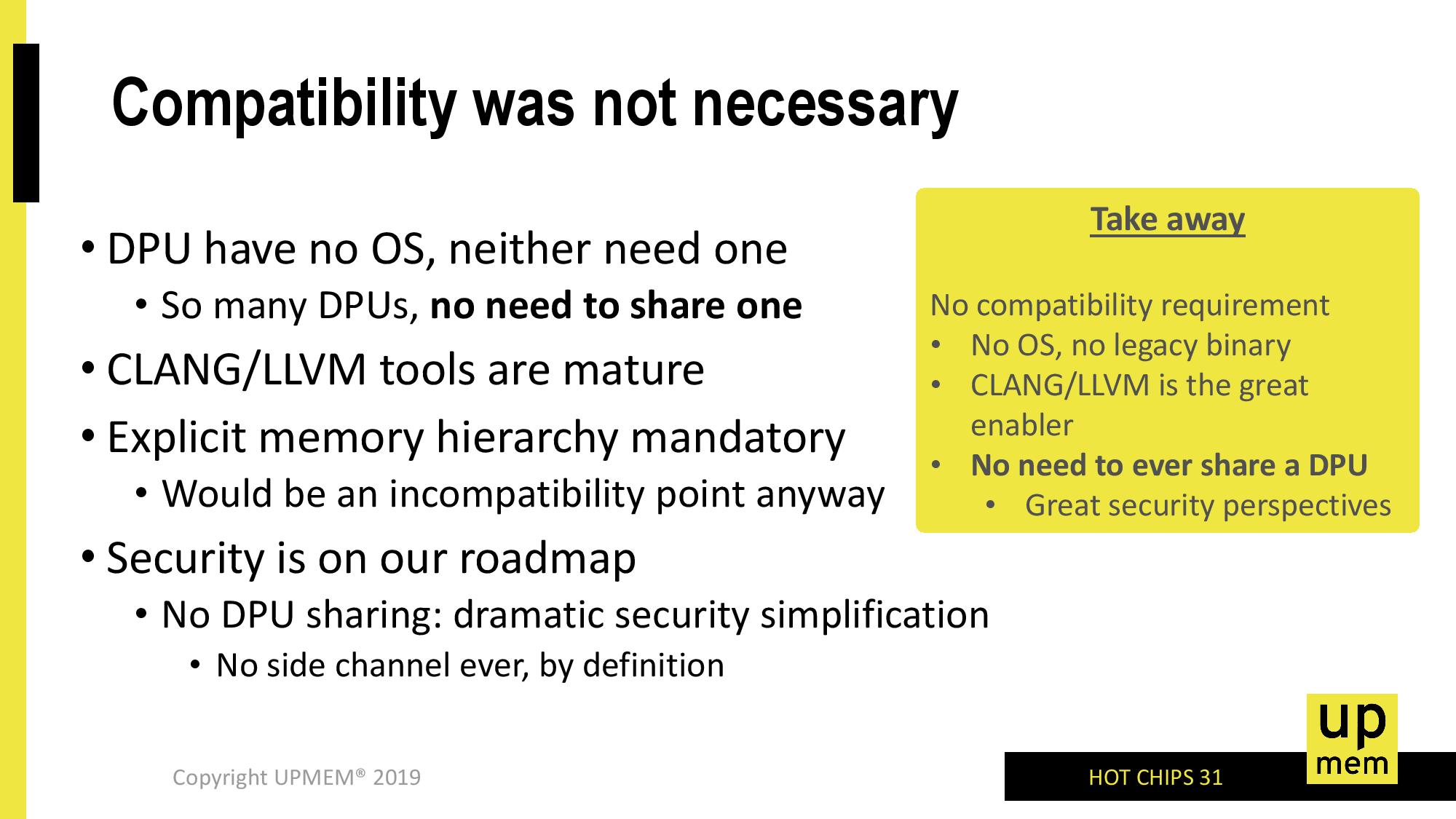
UPMEM states that Clang and LLVM tools are mature to manage DPU use through the compiler and provided APIs. Technically the DPUs have orchestration overhead as a result, and part of this is down to using DDR4 rather than a proprietary interface. UPMEM states that this orchestration management, such as bus width mismatches, address interleaving, the lack of cache coherent and the lack of hardware arbitration, is negligible compared to the work the DPU actually does. The APIs for managing this are available for x86, POWER 9, and ARM64.
Internally the DPU uses an optimized 32-bit ISA with triadic instructions, with non-destructive operand compute. As mentioned, the optimized ISA contains a range of typical instructions that can easily be farmed out to in-memory compute, such as SHIFT+ADD/SHIFT+SUB, basic logic (NAND, NOR, ORN, ANDN, NXOR), shift and rotate instructions, and even compute that requires intermediate values. The DPU supports bi-endianess, and is host OS agnostic.
The Goal
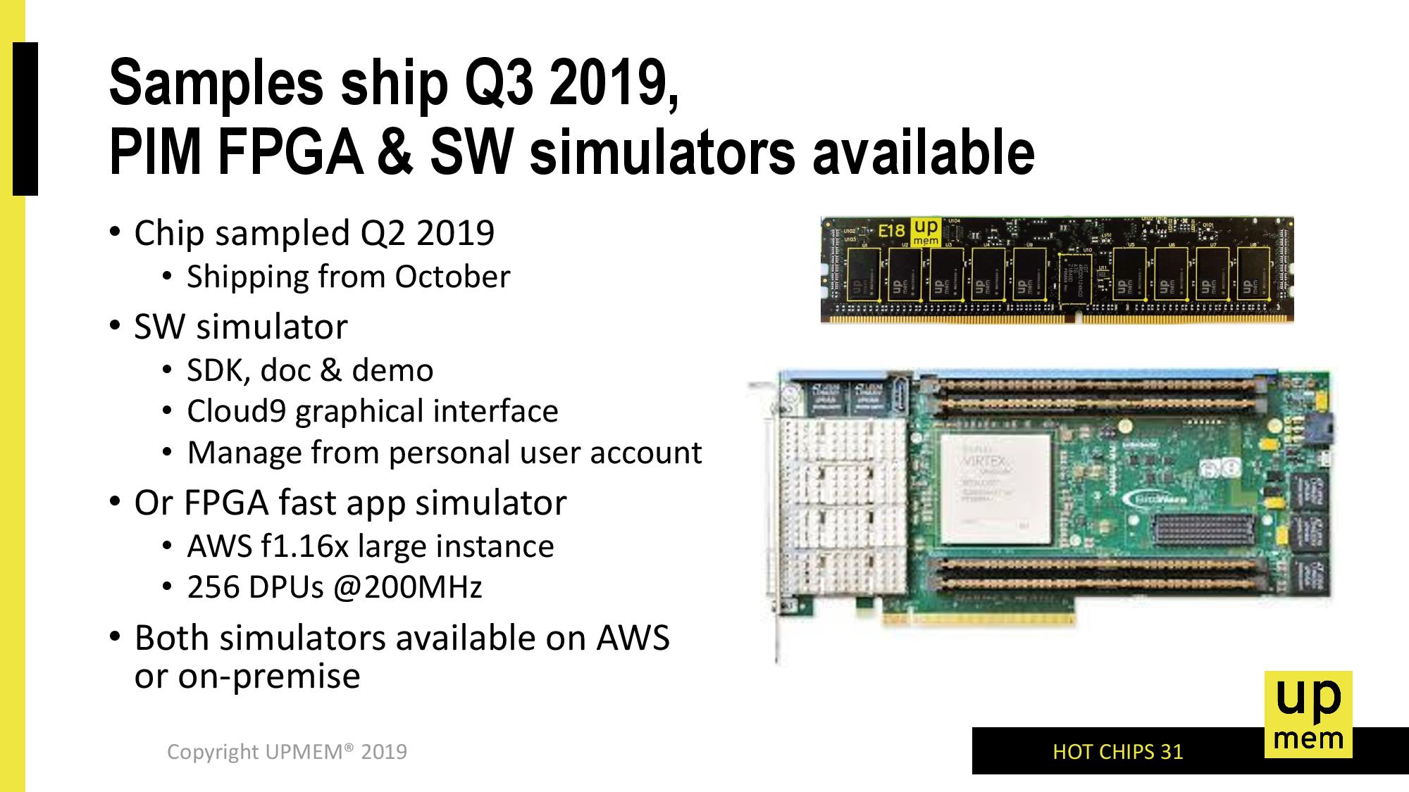
UPMEM is presenting its technology at Hot Chips as an attempt to attract potential customers, and is looking at mass production of its 8 GB memory modules in Q1, although early customers are already being sampled. The company is set to launch a sales office in the Bay Area during the second half of 2019.
The company is putting up impressive numbers for specific workloads, and to be honest, the question of in-memory compute is not really a question of if, but when. Even on the consumer side, there are some good examples where in-memory compute could help. I enjoyed going through UPMEM’s slide decks and looking at what they have to offer. It will be interesting to see other competing solutions come to the market, and how they approach the problem.
I will finish this article on one important note, however. Going up to 20W per 8 GB memory module is not a long-term solution. One of the disadvantages of moving compute away from the CPU is that you have to spend that compute power elsewhere, and a DRAM module isn’t usually the most ideal solution for that based on historic design (especially if doing the calculation is half as efficient). If a CPU socket can hold 150W, and a memory socket can do 20W, then you want most of the power consumed on the compute in the socket. In-memory compute is a good problem to solve, but ultimately it needs to be combined with on-CPU DRAM.


38 Comments
View All Comments
azazel1024 - Wednesday, August 21, 2019 - link
I prefer General In-Memory Processing. Just be careful of Last-level In-Memory Processing. I hear it can handicap your system if implemented wrong.winkingchef - Monday, August 19, 2019 - link
(This needs a #HotChips keyword tag)IMO this model of computing is the way the industry needs to go (pushing bits around from storage/memory to compute is wasteful of power).
HOWEVER, i also believe the adoption of this technology will be held back by the current mechanical/thermal assumptions around DRAM DIMMS which also drive electricals (spacing DIMMs out will create need for higher drive strength from the full rank of them to CPU). Someone will need to take a risk to adopt this on their server architecture.
Threska - Monday, August 19, 2019 - link
Basically diffusing a CPU into the space of a memory stick. Might be better to take the most used operations* in code and put those there.*Not to be confused with instructions. Too fine grained.
Elstar - Monday, August 19, 2019 - link
So many questions: what’s the security model? What’s the coherency model? How does virtual memory or virtualization in general interact with this? What happens when one DPU program needs data outside of its 64 MiB region?name99 - Saturday, August 24, 2019 - link
Yeah, these two issues (security and concurrency) are the immediate sticking points, and saying that a C-library hides them doesn't help much.An additional problem that hasn't been raised is the issue of physical address bit swizzling. Obviously this work happens at the physical address level, not virtual address; but it's worse than that. Right now physical address bits are rearranged in the memory to maximize DRAM utilization across all possible channels. So very low bits will target different memory controllers, then slightly less low bits will target ranks, and so on.
Meaning that I don't understand how this "No DPU sharing" provides real value. IF DPUs can only access their own data with no DPU cross traffic, then you're limited in how much damage you can do (but you're also massively limited in how much of value you can do...) But if DPUs can write to each other (necessary if you're going to support blits and memcopy, which would seem to be the first order win) then who cares about this "no sharing", how does it help?
Onur Mutlu's solution is much less sophisticated, but also seems a lot more practical. All that solution does is perform on-DRAM blits and memcopies, in essence by allowing the CPU to send instructions through the memory controller saying copy DRAM page at address A to DRAM page at address B. This gets you most of the win, while providing no security weirdness, and a very obvious chokepoint for how you perform the virtual to (controller, rank, bank, page) mapping rather than being a nightmare for generic code.
abufrejoval - Monday, August 19, 2019 - link
When I invented the concept perhaps ten years ago, I called it ‘computing memory’ and I was so glad, I found no matches for it on Google. But like with many other of my ideas, plenty of others had been there and actually done something about it, too.I was somewhat inspired by the Weitek Floating Point co-processor, an Intel i387 competitor which used a 64K memory segment while it only had perhaps 32 registers: It used the lowest significant address bit to encode one operation while writing the data, perhaps another while reading it: It very neatly solved the memory bottleneck between the CPU and the co-processor at the time, offering something like 4x the performance of Intel’s own.
Content addressable memory and the Linda Tuple space were other inspirations and I always wanted SQL-RAM, where the I’d put the WHERE clause into the address bits and then only retrieve matching data 😊.
I liked Micron's Automata Processor a lot, because it was a nice programming paradigm, good balance between problem solving power and logic overhead and excellent for formal proofs and unassailable by the likes of return oriented programming. Unfortunately they shelved that project.
HBM memory chip stacks offer free real-estate below the DRAM cells on the silicon die carrier, much like offices on the ground floor of a high-rise building with lots of elevators for the silicon tru vias (TSV). Even if the die carrier would be manufactured at a lower density, you’d have ample space for some simple logic at bandwidths much bigger than the CPU behind the chip multiplexing memory bus. I believe SK Hynix was at one point begging for engineers to come forward with ideas what to put there.
When the HP Memristor was supposed to offer 1000 layers and density at linear cost, it became very clear that general purpose CPUs simply wouldn’t be able to take advantage of that, much like a Morris Minor with 1000 BHP.
UPMEM is French I believe, I’ve heard about them for a long time, never seen a working chip yet. But computing memory is one of the few escape routes out of the von Neuman bottleneck.
abufrejoval - Monday, August 19, 2019 - link
Another idea was to use to expand on the row buffer also used for refresh. Use dual or tertiary buffers an a 'row ALU' that would operate on the entire memory row as a whole, e.g. for matching bit or byte patterns, then use some address bits to select transparent or operational access and write/modify the ALU row buffers.SaberKOG91 - Monday, August 19, 2019 - link
You didn't invent the idea: https://ieeexplore.ieee.org/document/592312I'm sure there are even early examples of this, but Patterson et. al were pretty prophetic in this arena.
abufrejoval - Tuesday, August 20, 2019 - link
Of course, I invented it, and all on my own, too!But as I mentioned (with a bit of irony between the lines) and you noticed, I just didn't invent it first nor did I manage to put it into physical implementation.
It's rather obviously the only open avenue of escape so idea duplication is natural.
I am actually more astonished at the lack of adoption over the last years, but silicon economics is still a game of scale.
But perhaps more importantly, those companies who's rising computing-power vs. value-of- computeratio is under the strongest pressure (GAFA/BATX), have found ways to push out the energy cost onto the client devices.
SaberKOG91 - Tuesday, August 20, 2019 - link
It has nothing to do with adoption or scale. The materials science for modern memory technologies took a long time to catch up, some of it didn't even exist until around decade ago, and only caught up because CMOS process tech lagged and slowed down the progress of everything else.It isn't selfish to push computing to client devices. These devices are faster to adopt optimized accelerators because they are now mostly mobile and battery restricted, which saves a tremendous amount of power overall, not just in the data-center.