Microchip Announces DRAM Controller For OpenCAPI Memory Interface
by Billy Tallis on August 5, 2019 8:00 AM EST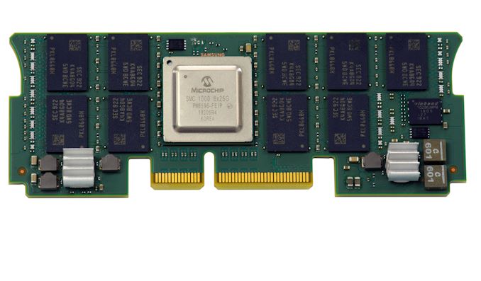
Microchip's subsidiary Microsemi is entering a new market with the introduction of the SMC 1000 8x25G Serial Memory Controller. This is a DDR4 DRAM controller that connects to host processors using the OpenCAPI-derived Open Memory Interface (OMI), a high-speed differential serial link running at 25Gbps per lane. The purpose is to enable servers to scale to much higher memory capacities by attaching DRAM through serial links with much lower pin counts than traditional parallel DDR interfaces.
OpenCAPI is one of several competing high-speed interconnect standards that seek to go beyond the performance and feature set of PCI Express. The first two CAPI standards were built atop PCIe 3.0 and 4.0 and offered a lower-latency, cache-coherent protocol. Version 3 gained the Open- prefix by moving control of the spec from IBM to a new consortium, and OpenCAPI 3.0 abandons its PCIe underpinnings in favor of a new 25Gbps link. A subset of OpenCAPI 3.1 has been dubbed Open Memory Interface, and provides a media-agnostic but low-latency protocol for accessing memory. There's open IP available for implementing the host or target side of this interface, and a growing ecosystem of commercial tools for design verification.
The Microchip SMC 1000 8x25G unsurprisingly uses an 8-lane Open Memory Interface connection to the host, and on the downstream side it has a single-channel DDR4-3200 controller with ECC and support for four ranks of memory. The SMC 1000 at heart is a SERDES with a few extra features, allowing a CPU to use an 84-pin connection in place of a 288-pin DIMM interface, without sacrificing bandwidth and only incurring an extra 4ns of latency compared to LRDIMMs attached to an on-CPU memory controller. The chip itself is a 17x17 mm package with typical power consumption below 1.7W, and it supports dynamically dropping down to four or two lanes on the OMI link to save power when the full 25GB/s isn't needed.
In principle, the DRAM interface of the SMC 1000 could fan out to traditional DIMM slots, but the preferred way to use the chip will be to put the controller and a fixed amount of DRAM together onto a module called a Differential DIMM. These DDIMMs will use the same SFF-TA-1002 connector as EDSFF/Ruler SSDs, and the modules will be 85mm long compared to 133mm LRDIMMs. Both 1U and 2U height DDIMM form factors are in the process of being standardized. Microchip already has Samsung, Micron and SMART Modular on board to manufacture DDIMMs using the SMC 1000 controller, with initial capacities ranging from 16GB to 256GB per module.
On the host side, the first platforms to support Open Memory Interface will be POWER9 processors from IBM, and they are expected to announce more details later this month at their OpenPOWER Summit. From IBM's perspective, supporting Open Memory Interface allows them to include more memory channels on the same size die, and provides a forward-compatible upgrade path to DDR5 and NVDIMMs or other memory technologies since the details of those interfaces are now handled on the DDIMM instead of on the CPU.
Microchip will be showing off the SMC 1000 8x25G at Flash Memory Summit this week, and will be giving a keynote presentation Wednesday morning.


17 Comments
View All Comments
Kevin G - Monday, August 5, 2019 - link
Intel only had four SMI buses on the Xeon E7 that would go to the memory buffer chips but from there, the memory buffer would fan out to two traditional DDR3 or DDR4 channels. So the result was effectively an 8 channel DDR3/DDR4 setup. A fully decked out quad socket server of that era with 128 GB DIMMs could support 12 TB of RAM. These are still desirable today as they don't incur the memory capacity tax that Intel has artificially placed on Xeon Scalable chips.Kevin G - Monday, August 5, 2019 - link
Being able to fan out to traditional DIMMs maybe the higher capacity option if each of those chips can support two DDR4 LR-DIMMs. If a board maker wanted to go for pure capacity, I'd expect the host POWER9+ to have something like 64 OMI memory channels but if these SMC 1000 chips are able to operate across one single OMI link. That'd be 128 traditional DIMMs per socket and at 256 GB per LR-DIMM, a 32 TB per socket capacity. Sixteen sockets like that would permit a 0.5 PB capacity in a single logical system. Lots of what-ifs to get there and the physical layout would be a thing of logistical nightmares, but IBM could just be aiming to be the first to such capacities regardless if it would be realistically obtainable.**Though for those who only care about memory capacity, have money growing tree, and no regards to performance, a 1.5 GB system might be possible on the x86 side through a custom system via HPE. They bought SGI and their NUMAlink architecture for inclusion in future SuperDome systems. That scaled up to 256 sockets under the SGI banner but the newer models under HP are only listed up to 32. However, at 256 sockets wtih Xeon SP with 12 DIMM slots each and only using 512 GB Optane DIMMs (bye-bye performance), that'd get you a 1.5 PB capacity. Again, lots of what-ifs and speculation to make such a box happen.
rbanffy - Wednesday, August 21, 2019 - link
IBM plays long term. They've been playing the 360+ mainframe since the 60's and profiting wonderfully from it. AFAIK, current z boxes (more like "fridges") already uses something like this and this would allow to build machines where the memory doesn't need to be so tightly coupled to a CPU socket. Think processor and memory in separate drawers, allowing for logical partitioning into multiple smaller "machines" or a single humongous consolidated monsterPeachNCream - Monday, August 5, 2019 - link
A multiple lane serial link is a parallel link.anonomouse - Monday, August 5, 2019 - link
Not exactly - different requirements on inter-lane skew vs a true parallel link like DDR, which has 64 parallel links which all must clock together. The 8 serial lanes probably each have their own independent clocks, and as serial links there's not much worry about skew within each link.azfacea - Monday, August 5, 2019 - link
72 with eccMojArch - Monday, August 5, 2019 - link
hiI am newbie to this stuff can some one point me what exactly they try to do?
Is it like conventional ram? or some thing else?