AMD Rome Second Generation EPYC Review: 2x 64-core Benchmarked
by Johan De Gelas on August 7, 2019 7:00 PM ESTMemory Subsystem: Latency
AMD chose to share a core design among mobile, desktop and server for scalability and economic reasons. The Core Complex (CCX) is still used in Rome like it was in the previous generation.
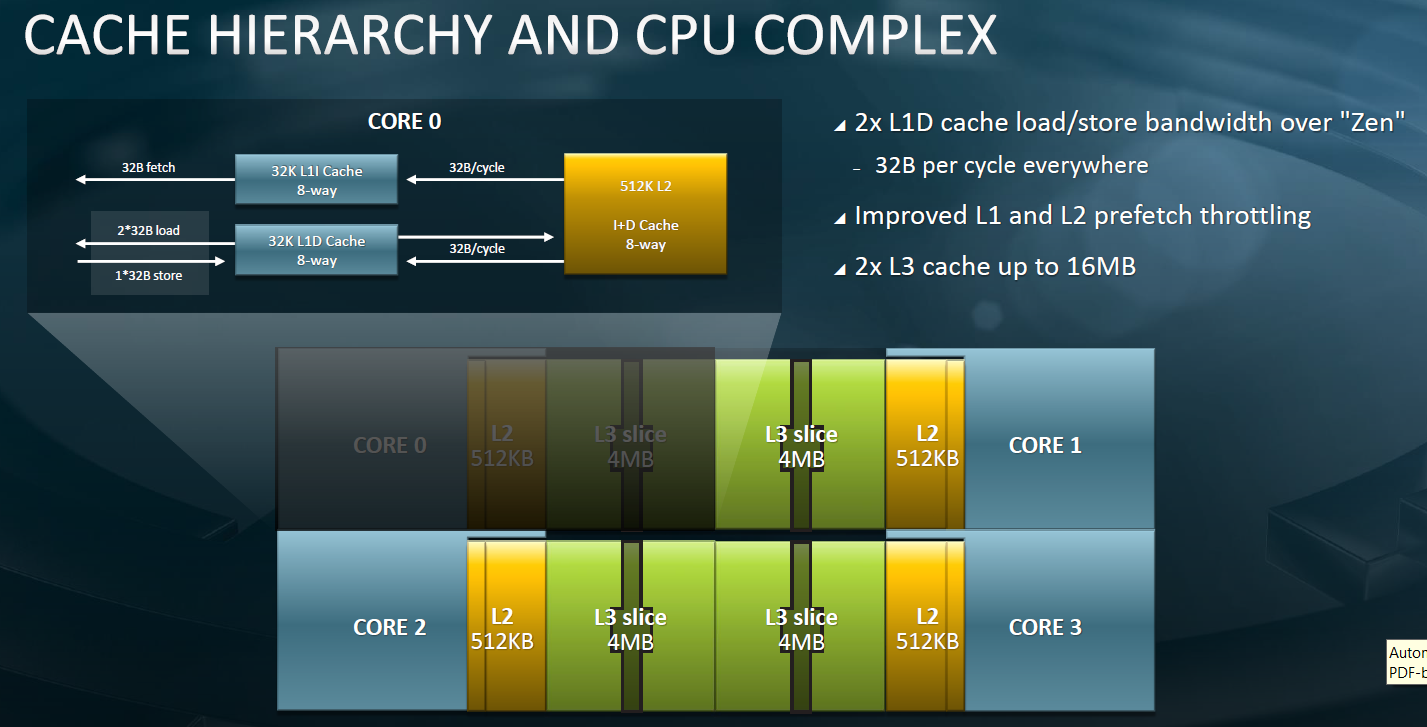
What has changed is that each CCX communicates with the central IO hub, instead of four dies communicating in 4 node NUMA layout (This option is still available to use via the NPS4 switch, keeping each CCD local to its quadrant of the sIOD as well as those local memory controllers, avoiding hops between sIOD quadrants which encour a slight latency penalty). So as the performance of modern CPUs depends heavily on the cache subsystem, we were more than curious what kind of latency a server thread would see as it accesses more and more pages in the cache hierarchy.
We're using our own in-house latency test. In particular what we're interested in publishing is the estimated structural latency of the processors, meaning we're trying to account for TLB misses and disregard them in these numbers, except for the DRAM latencies where latency measurements get a bit more complex between platforms, and we revert to full random figures.
| Mem Hierarchy |
AMD EPYC 7742 DDR4-3200 (ns @ 3.4GHz) |
AMD EPYC 7601 DDR4-2400 (ns @ 3.2GHz) |
Intel Xeon 8280 DDR-2666 (ns @ 2.7GHz) |
|
| L1 Cache | 32KB 4 cycles 1.18ns |
32KB 4 cycles 1.25ns |
32KB 4 cycles 1.48ns |
|
| L2 Cache | 512KB 13 cycles 3.86ns |
512KB 12 cycles 3.76ns |
1024KB 14 cycles 5.18ns |
|
| L3 Cache | 16MB / CCX (4C) 256MB Total ~34 cycles (avg) ~10.27 ns |
16MB / CCX (4C) 64MB Total |
38.5MB / (28C) Shared ~46 cycles (avg) ~17.5ns |
|
| DRAM 128MB Full Random |
~122ns (NPS1) ~113ns (NPS4) |
~116ns |
~89ns |
|
| DRAM 512MB Full Random |
~134ns (NPS1) ~125ns (NPS4) |
~109ns |
||
Update 2019/10/1: We've discovered inaccuracies with our originally published latency numbers, and have subsequently updated the article with more representative figures with a new testing tool.
Things get really interesting when starting to look at cache depths beyond the L2. Naturally Intel here this happens at 1MB while for AMD this is after 512KB, however AMD’s L2 has a speed advantage over Intel’s larger cache.
Where AMD has an ever more clearer speed advantage is in the L3 caches that are clearly significantly faster than Intel’s chips. The big difference here is that AMD’s L3’s here are only local to a CCX of 4 cores – for the EPYC 7742 this is now doubled to 16MB up from 8MB on the 7601.
Currently this is a two-edged sword for the AMD platforms: On one hand, the EPYC processors have significantly more total cache, coming in at a whopping 256MB for the 7742, quadruple the amount over the 64MB of the 7601, and a lot more than Intel’s platforms, which come in at 38.5MB for the Xeon 8180, 8176, 8280, and a larger 55MB for the Xeon E5-2699 v4.
The disadvantage for AMD is that while they have more cache, the EPYC 7742 rather consist of 16 CCX which all have a very fast 16 MB L3. Although the 64 cores are one big NUMA node now, the 64-core chip is basically 16x 4 cores, each with 16 MB L3-caches. Once you get beyond that 16 MB cache, the prefetchers can soften the blow, but you will be accessing the main DRAM.
A little bit weird is the fact that accessing data that resides at the same die (CCD) but is not within the same CCX is just as slow as accessing data is on a totally different die. This is because regardless of where the other CCX is, whether it is nearby on the same die or on the other side of the chip, the data access still has to go through the IF to the IO die and back again.
Is that necessarily a bad thing? The answer: most of the time it is not. First of all, in most applications only a low percentage of accesses must be answered by the L3 cache. Secondly, each core on the CCX has no less than 4 MB of L3 available, which is far more than the Intel cores have at their disposal (1.375 MB). The prefetchers have a lot more space to make sure that the data is there before it is needed.
But database performance might still suffer somewhat. For example, keeping a large part of the index in the cache improve performance, and especially OLTP accesses tend to quite random. Secondly the relatively slow communication over a central hub slow down synchronization communication. That is a real thing is shown by the fact that Intel states that the OLTP hammerDB runs 60% faster on a 28-core Intel Xeon 8280 than on EPYC 7601. We were not able to check it before the deadline, but it seems reasonable.
But for the vast majority of these high-end CPUs, they will be running many parallel applications, like running microservices, docker containers, virtual machines, map/reducing smaller chunks of data and parallel HPC Jobs. In almost all cases 16 MB L3 for 4 cores is more than enough.
Although come to think of it, when running an 8-core virtual machine there might be small corner cases where performance suffers a (little) bit.
In short, AMD leaves still a bit of performance on table by not using a larger 8-core CCX. We await to see what happens in future platforms.


180 Comments
View All Comments
ET - Thursday, August 8, 2019 - link
I found the EPYC 7262 the most interesting SKU. By L3 cache size, that would be 4 chiplets, each offering only 2 cores. From the specs it looks like AMD has no shortage of 4 core chiplets, but I didn't expect 2 core chiplets.Rudde - Friday, August 9, 2019 - link
L3 cache is shared inside a CCX (4 cores), which suggests that every CCX has only one core available, but 16MB of L3 cache. I.e. every core has private L3 cache.colonelclaw - Thursday, August 8, 2019 - link
But can it serve Crysis Battle Royale?shing3232 - Thursday, August 8, 2019 - link
I am pretty sure it can lolBigMamaInHouse - Thursday, August 8, 2019 - link
@ Johan De Gelas will u test @240W TDP config?JohanAnandtech - Thursday, August 8, 2019 - link
Elaborate your interest in that, as it is only tad higher than the official 225W TDP?BigMamaInHouse - Thursday, August 8, 2019 - link
AMD is offering 225W/240W TDP option in bios to it's customers and lets them to decide if to go with better cooling and use 240W or stay at 225W, even though it looks small increase- in reality it should offer almost 10% more power headroom to the CPU chiplets -if you consider that the 225W is including ~55W for I/O die, so extra 15W for the chiplets alone should offer nice bump in clocks.Gondalf - Thursday, August 8, 2019 - link
Strange.....the article forgot Cooper Lake, out in Q4 this year and at major customers (for revenue) from at least two quarters. Same applies to Ice Lake SP that is in evaluation to OEMs right now.From the article looks like Intel is sleeping, but it is not at all. Ummm maybe Intel is snobbing some guys here not giving samples to test?? or informations to share??
Bet Intel have to argue about the test suite or about compiler settings.........
JohanAnandtech - Thursday, August 8, 2019 - link
Because Cooper Lake is still "warmed up Skylake" (unless I missed something). AFAIK it is Cascade Lake with 8 mem channels - so the 56-core socketed will probably be still in the 350-400W TDP range. So the SPEC benchmarks will look better, but getting that kind of server running inside your datacenter does not look very attractive: complex and thus expensive boards, high cooling and power distribution required. Looks like a chip that wins back benchmarks, but is too much hassle to roll out in high quantities.Null666666 - Friday, August 9, 2019 - link
Wondering when 4-8 socket ice lake is due.