The AMD 3rd Gen Ryzen Deep Dive Review: 3700X and 3900X Raising The Bar
by Andrei Frumusanu & Gavin Bonshor on July 7, 2019 9:00 AM ESTCache Hierarchy Changes: Double L3, Faster Memory
Among the biggest changes of the Ryzen 3000, alongside the improved core microarchitecture, is the chip’s overall cache hierarchy. The new chiplet houses CCXes with double the amount of L3, now 16MB instead of 8MB.
Furthermore the chiplet design with the introduction of the cIO die which houses the new memory controllers are undoubtedly going to have an impact on the memory latency and performance of the overall chip.
On the memory controller side particularly, AMD promises a wholly revamped design that brings new support for a whole lot faster DDR4 modules, with the chip coming by default categorized as supporting DDR4-3200, which is a bump over the DDR-2933 support of the Ryzen 2000 series.
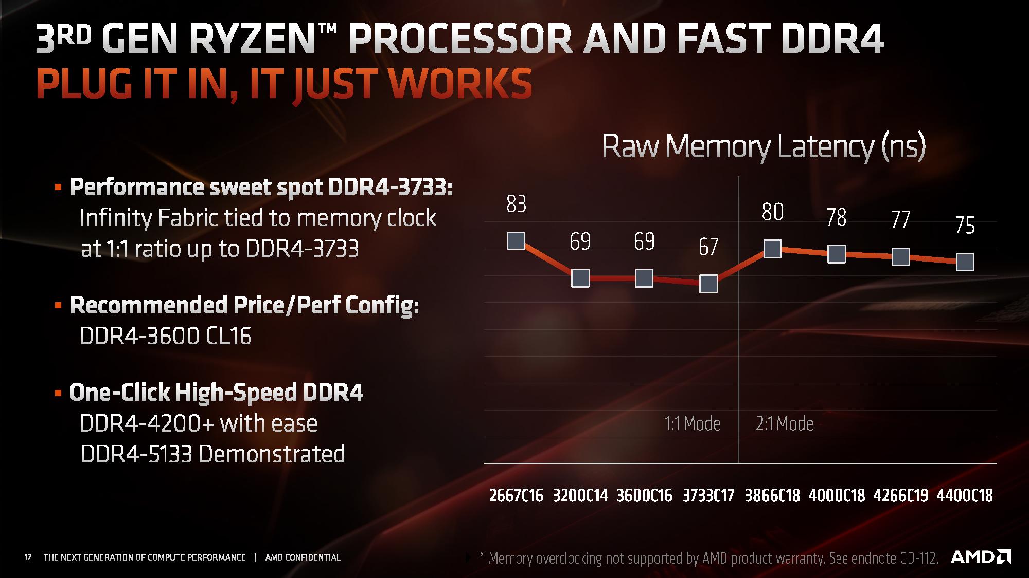
AMD had published an interesting slide in regards to the new faster DDR support that went well above the officially supported 3200 speeds, with AMD claiming that the new controllers are able to support up to DDR4-4200 with ease and overclocking being possible to achieve ever higher speeds. However there’s a catch: in order to support DDR4 above 3600, the chip will automatically change the memory controller to infinity fabric clock ratio from being 1:1 to 2:1.
Whilst this doesn’t bottleneck the bandwidth of the memory to the cores as the new microarchitecture has now doubled the bus width of the Infinity Fabric to 512 bits, it does add a notable amount of cycles to the overall memory latency, meaning for the very vast majority of workloads, you’re better off staying at or under DDR4-3600 with a 1:1 MC:IF ratio. It’s to be noted that it’s still possible to maintain this 1:1 ratio by manually adjusting it at higher MC speeds, however stability of the system is no longer guaranteed as you’re effectively overclocking the Infinity Fabric as well in such a scenario.
For this article we didn’t have enough time to dive into the scaling behaviour of the different DRAM speeds, what we did investigate is a more architectural question of how exactly the new chiplet and cIO die architecture has impacted Zen2’s memory latency and memory performance.
To give better insights, we’re using my custom memory latency test that I use for mobile SoC testing and first covered in our review of the Galaxy S10+ and its two SoCs. Memory latency testing nowadays is a complicated topic as microarchitectures advance at a rapid rate, and in particular prefetchers can cause for sometimes misleading figures. Similarly, more brute-force approaches such as full random tests contain a lot of TLB miss latencies which don’t represent the actual structural latency of the system. Our custom latency suite thus isn’t a single one-number-fits-all test but rather a collection of tests that expose more details of the memory behaviour of the system.
The figures published on this page are run on DDR4-3200CL16 on the Ryzen 3900X and 2700X at timings of 16-16-16-36, and the i9-9900K was run with similar DDR4-3200CL16 at timings of 16-18-18-36.
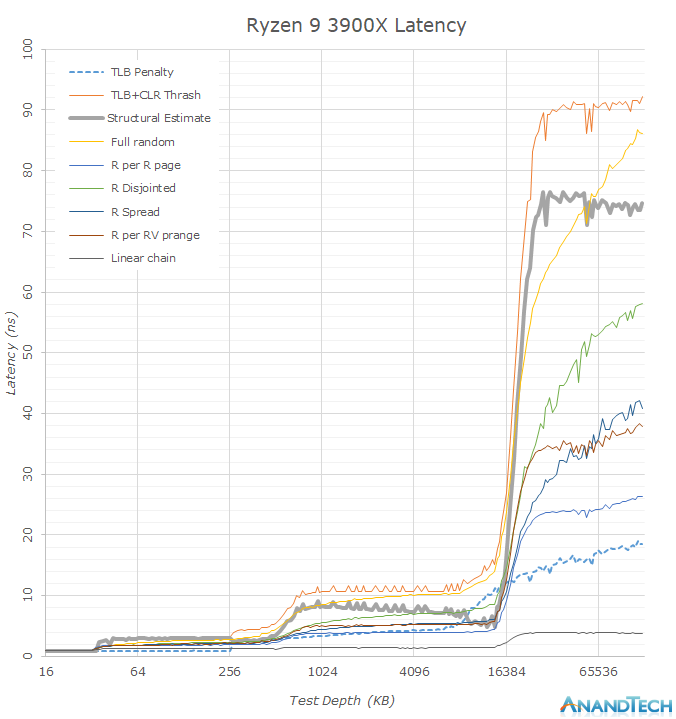
Looking at the memory latency curves in a linear plotted graph, we see that there’s some larger obvious differences between the new Ryzen 3900X and the Ryzen 2700X. What immediately catches the eye when switching between the two results is the new 16MB L3 cache capacity which doubles upon the 8MB of Zen1. We have to remind ourselves that even though the whole chip contains 64MB of L3 cache, this is not a unified cache and a single CPU core will only see its own CCX’s L3 cache before going into main memory, which is in contrast to Intel’s L3 cache where all the cores have access to the full amount.
Before going into more details in the next graph, another thing that is obvious is that seemingly the 3900X’s DRAM latency is a tad worse than the 2700X’s. Among the many test patterns here the one to note is the “Structural Estimate” curve. This curve is actually a simple subtraction of the TLB+CLR Thrash tests minus the TLB Penalty figure. In the former, we’re causing as much cache-line replacement pressure as possible by repeatedly hitting the same cacheline within each memory page, also repeatedly trying to miss the TLB. In the latter, we’re still hitting the TLB heavily, but always using a different cache-line and thus having a minimum of cache-line pressure, resulting in an estimate of the TLB penalty. Subtracting the latter from the former gives us a quite good estimate of the actual structural latency of the chip and memory.
Now the big question is, why do it this way? I’ve found that with increasingly better prefetchers, it’s getting difficult in getting good memory latency numbers. Whilst it’s possible to just outright disable prefetchers on some platforms, that avenue isn’t always available.
Precisely when looking at the other various patterns in the graph, we’re seeing quite a large difference between the 3900X and the 2700X, with the 3900X showcasing notably lower latencies in a few of them. These figures are now a result of the new Zen2’s improved prefetchers which are able to better recognize patterns and pull out data from DRAM before the CPU core will handle that memory address.
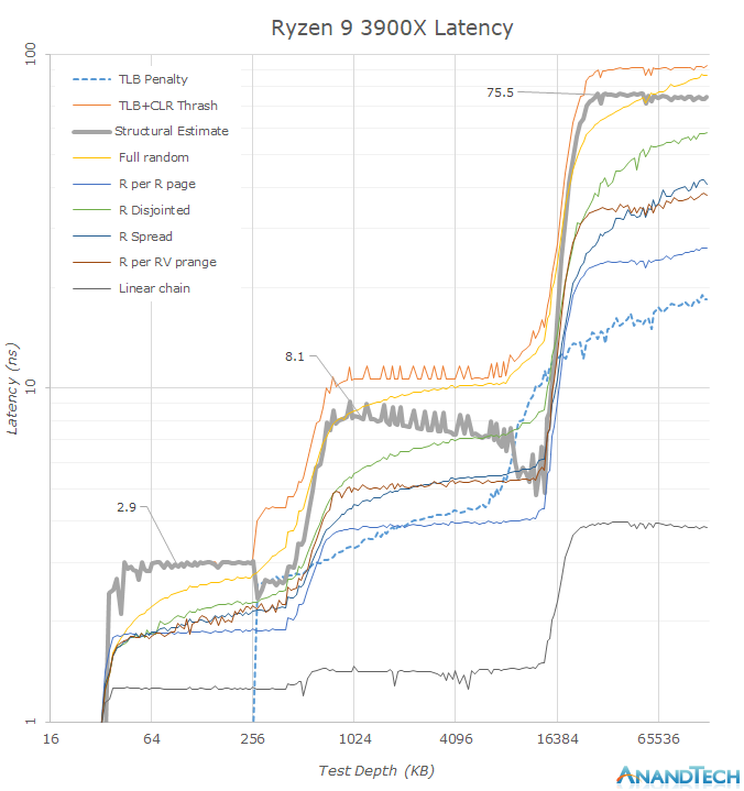
Plotting the same data on a logarithmic graph, we better see some of the details.
In terms of the DRAM latency, it seems that the new Ryzen 3900X has regressed by around 10ns when compared to the 2700X (Note: Just take into the leading edge of the “Structural Estimate” figures as the better estimate) with ~74-75.5ns versus ~65.7ns.
It also looks like Zen2’s L3 cache has also gained a few cycles: A change from ~7.5ns at 4.3GHz to ~8.1ns at 4.6GHz would mean a regression from ~32 cycles to ~37 cycles. Such as change however was to be expected since doubling of the L3 cache structure has to come with some implementation compromises as there’s never just a free lunch. Zen2’s L3 cache latency is thus now about the same as Intel’s – while it was previously faster on Zen+.
Further interesting characteristics we see here is the increase of the capacity of the L2 TLB. This can be seen in the “TLB Penalty” curve, and the depth here corresponds to AMD’s published details of increasing the structure from 1536 pages to 2048 pages. It’s to be noted that the L3 capacity now exceeds the capacity of the TLB, meaning a single CPU core will have only the best access latencies to up to 8MB in the cache before starting to have to page-walk. A similar behaviour we see in the L2 cache where the L1 TLB capacity only covers 256KB of the cache before having to look up entries in the L2 TLB.
Another very interesting characteristic of AMD’s microarchitecture which contrasts Intel’s, is the fact that AMD prefetches all patterns into the L2 cache, while Intel only does so for the nearest cache-line. Such a behaviour is a double-edged sword, on one hand AMD’s cores have can have better latencies to needed data, but on the other hand in the case of a unneeded prefetch, it puts a lot more pressure on the L2 cache capacity, and could in effect counter-act some of the benefits of having double the capacity over Intel’s design.
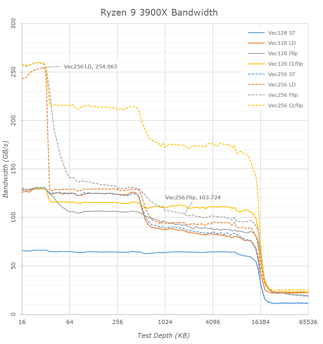
Switching over to the memory bandwidth of the cache hierarchy, there’s one obvious new chance in the 3900X and Zen2: the inclusion of 256-bit wide datapaths. The new AGU and path changes mean that the core is able to now handle 256-bit AVX instruction once per cycle which is a doubling over the 128-bit datapaths of Zen and Zen+.
So while the bandwidth of 256-bit operations on the Ryzen 2700X looked identical to the 128-bit variants, the wider ops now on Zen2 effectively double the bandwidth of the core. This bandwidth doubling is evident in the L1 cache (The flip test is equal to a memory copy test), however the increase is only about 20% for the L2 and L3 caches.
There’s an interesting juxtaposition between AMD’s L3 cache bandwidth and Intel’s: AMD essentially has a 60% advantage in bandwidth, as the CCX’s L3 is much faster than Intel’s L3 when accessed by a single core. Particularly read-write modifications within a single cache-line (CLflip test) are significantly faster in both the L2 and L3 caches when compared to Intel’s core design.
Deeper into the DRAM regions, however we see that AMD is still lagging behind Intel when it comes to memory controller efficiency, so while the 3900X improves copy bandwidth from 19.2GB/s to 21GB/s, it still remains behind the 9900K’s 22.9GB/s. The store bandwidth (write bandwidth) to memory is also a tad lower on the AMD parts as the 3900X reaches 14.5GB/s versus Intel’s 18GB/s.
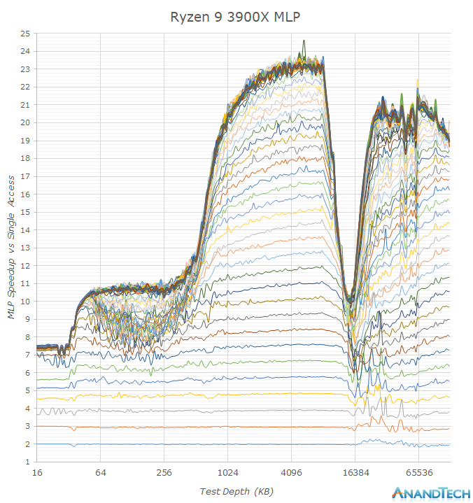
One aspect that AMD excels in is memory level parallelism. MLP is the ability for the CPU core to “park” memory accesses when they are missing the caches, and wait on them to return back later. In the above graph we see increasing number of random memory accesses depicted as the stacked lines, with the vertical axis showcasing the effective access speedup in relation to a single access.
Whilst both AMD and Intel’s MLP ability in the L2 are somewhat the same and reach 12 – this is because we’re saturating the bandwidth of the cache in this region and we just can’t go any faster via more accesses. In the L3 region however we see big differences between the two: While Intel starts off with around 20 accesses at the L3 with a 14-15x speedup, the TLBs and supporting core structures aren’t able to sustain this properly over the whole L3 as it’s having to access other L3 slices on the chip.
AMD’s implementation however seems to be able to handle over 32 accesses with an extremely robust 23x speedup. This advantage actually continues on to the DRAM region where we still see speed-ups up to 32 accesses, while Intel peaks at 16.
MLP ability is extremely important in order to be able to actually hide the various memory hierarchy latencies and to take full advantage of a CPU’s out-of-order execution abilities. AMD’s Zen cores here have seemingly the best microarchitecture in this regard, with only Apple’s mobile CPU cores having comparable characteristics. I think this was very much a conscious design choice of the microarchitecture as AMD knew their overall SoC design and future chiplet architecture would have to deal with higher latencies, and did their best in order to minimise such a disadvantage.
So while the new Zen2 cores do seemingly have worse off latencies, possibly a combined factor of a faster memory controller (faster frequencies could have come at a cost of latency in the implementation), a larger L3 but with additional cycles, it doesn’t mean that memory sensitive workloads will see much of a regression. AMD has been able to improve the core’s prefetchers, and average workload latency will be lower due to the doubled L3, and this is on top the core’s microarchitecture which seems to have outstandingly good MLP ability for whenever there is a cache miss, something to keep in mind as we investigate performance further.


447 Comments
View All Comments
John_M - Sunday, July 7, 2019 - link
Yes. The integrated memory controller is on the IO die, which is part of the Ryzen SoC, not the chipset.BushLin - Monday, July 8, 2019 - link
Right now, there's no indication what CL / timings are applied to all the other systems. CL16 is indeed bottom of the barrel for DDR-3200, you would hope there's no shenanigans with Intel getting CL12 DDR-2666. Why not just run all the systems with the same DDR-3200, it's not like they can't do it.profiaudi - Wednesday, July 10, 2019 - link
Not to be too rude, but the IMC is on the io chipLet, not the chipSet. The chipset actually has an important role for the memory speed, in that a chipset defines a platform and a platform imposes requirements on the power supply and trace routing. While the IMC in 3rd gen can handle 3200MT/s+ completely fine, it is guaranteed to do so only one X570. Anything older is a dice roll as the boards were not designed for such speeds (not a requirement for the older platform).waja - Tuesday, July 23, 2019 - link
Do you know george stevenson story?He earn 3657$ every month at home just working few hours on internet see more by open this connection and click home button.FOR MORE INFORMATION COPY THIS SITE.......... www.online-3.comAndrei Frumusanu - Sunday, July 7, 2019 - link
Just as note for those who haven’t been following: This review wasn’t written by our usual resident CPU editor, Dr Ian Cutress as he unfortunately the timing didn’t work out. We only had a few days time with the new Ryzen CPUs, as such, you might noticed a few bits and pieces missing in our article that we’ll try to address in the next hours and days. We’ll be trying to update the piece with more information and data as soon as we can. Thanks.Also huge thanks to Gavin Bonshor who actually did all the testing and collected all the data for this review, thumb up to him.
plonk420 - Sunday, July 7, 2019 - link
hoping a speedy recovery for him! loved his video with Wendell!loving the article, too. don't suppose you could test cross-CCX latency?
plonk420 - Sunday, July 7, 2019 - link
e.g. pcper.com/2017/06/the-intel-core-i9-7900x-10-core-skylake-x-processor-review/3/main interest is if it is low enough to be harnessed by RPCS3 (PS3 emulator)
ballsystemlord - Sunday, July 7, 2019 - link
CCX benchmarks would be nice.IF power benchmarks were also done last time and probably in the works.
shakazulu667 - Sunday, July 7, 2019 - link
Are Intel results with or without spectre et al mitigations?Ryan Smith - Sunday, July 7, 2019 - link
They are with Spectre and Meltdown mitigations. They are not new enough results to include anything for Fallout/ZombieLoad.