AMD Zen 2 Microarchitecture Analysis: Ryzen 3000 and EPYC Rome
by Dr. Ian Cutress on June 10, 2019 7:22 PM EST- Posted in
- CPUs
- AMD
- Ryzen
- EPYC
- Infinity Fabric
- PCIe 4.0
- Zen 2
- Rome
- Ryzen 3000
- Ryzen 3rd Gen
AMD Zen 2 Microarchitecture Overview
The Quick Analysis
At AMD’s Tech Day, on hand was Fellow and Chief Architect Mike Clark to go through the changes. Mike is a great engineer to talk to, although what always amuses me (for any company, not just AMD) is that engineers that talk about the latest products coming to market are already working one, two, or three generations ahead at the company. Mike remarked that it took him a while to think back to the specific Zen+ to Zen 2 changes, while his mind internally is already several generations down the line.
An interesting element to Zen 2 is around the intention. Initially Zen 2 was merely going to be a die shrink of Zen+, going from 12nm down to 7nm, similar to what we used to see with Intel in its tick-tock model for the initial part of the century. However, based on internal analysis and the time frame for 7nm, it was decided that Zen 2 would be used as a platform for better performance, taking advantage of 7nm in multiple ways rather than just redesigning the same layout on a new process node. As a result of the adjustments, AMD is promoting a +15% IPC improvement for Zen 2 over Zen+.
When it comes down to the exact changes in the microarchitecture, what we’re fundamentally looking at is still a similar floorplan to what Zen looks like. Zen 2 is a family member of the Zen family, and not a complete redesign or different paradigm on how to process x86 – as will other architectures that have familial updates, Zen 2 affords a more efficient core and a wider core, allowing better instruction throughput.
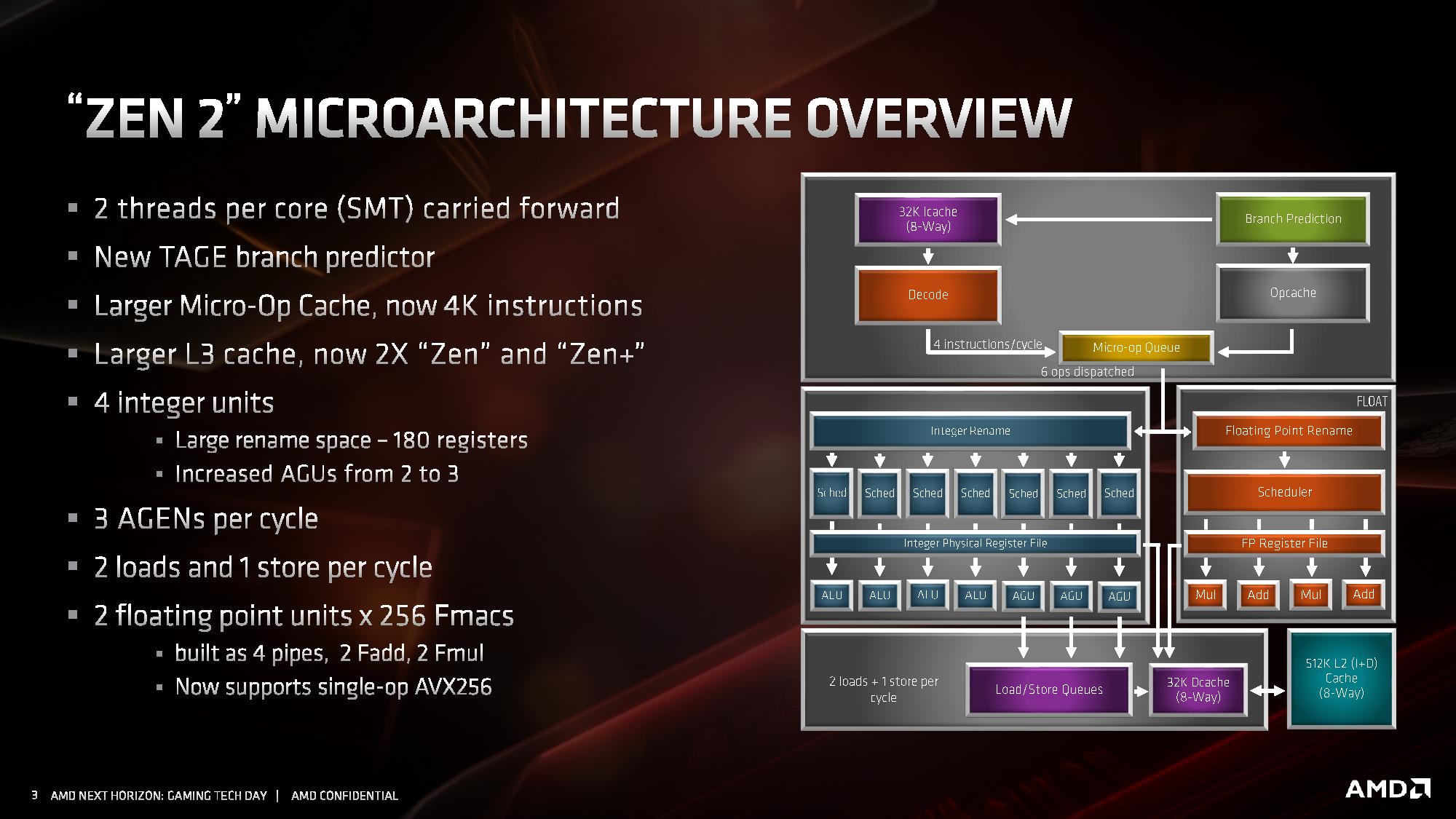
At a high level, the core looks very much the same. Highlights of the Zen 2 design include a different L2 branch predictor known as a TAGE predictor, a doubling of the micro-op cache, a doubling of the L3 cache, an increase in integer resources, an increase in load/store resources, and support for single-operation AVX-256 (or AVX2). AMD has stated that there is no frequency penalty for AVX2, based on its energy aware frequency platform.
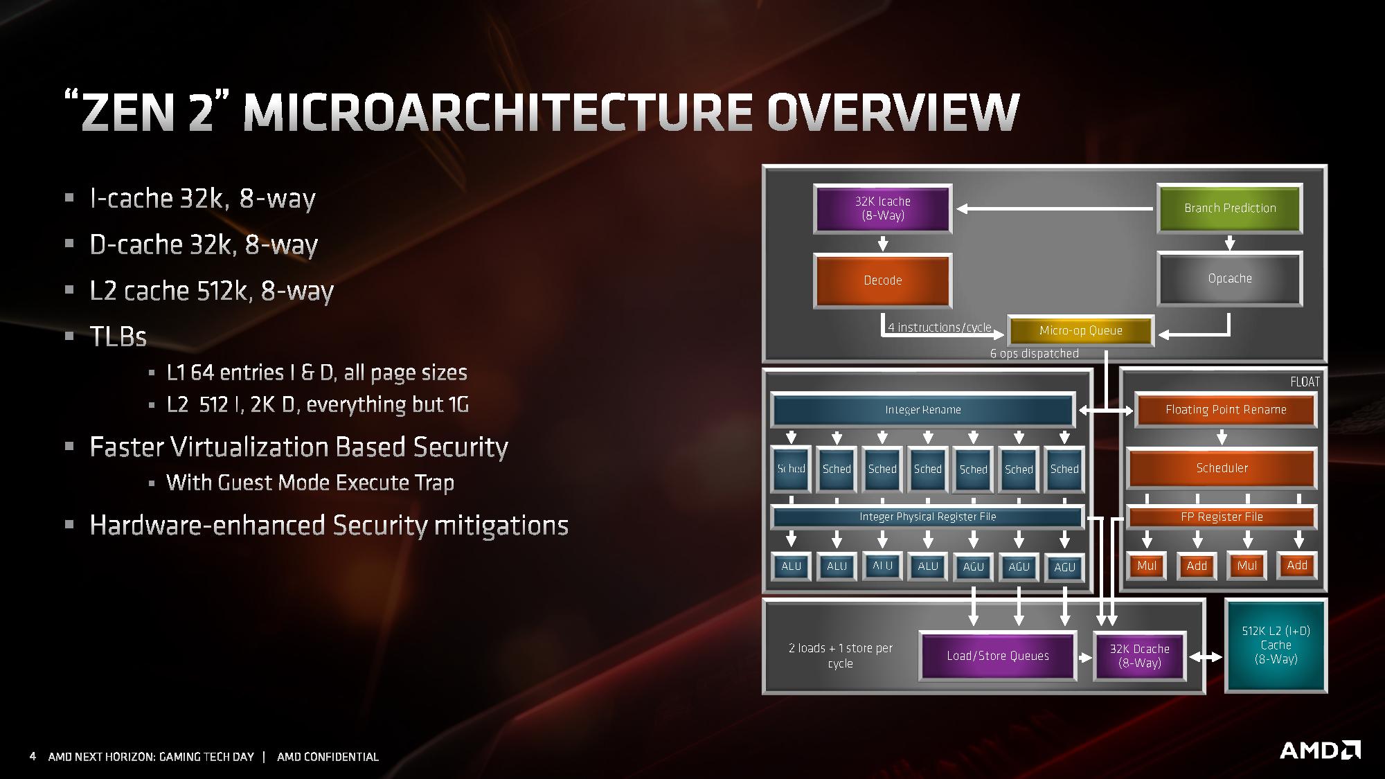
AMD has also made adjustments to the cache system, the most notable being for the L1 instruction cache, which has been halved to 32 kB, but associativity has doubled. This change was made for important reasons, which we’ll go into over the next pages. The L1 data cache and L2 caches are unchanged, however the translation lookaside buffers (TLBs) have increased support. AMD also states that it has added deeper virtualization support with respect to security, helping enable features further down the pipeline. As mentioned previously in this article, there are also security hardening updates.
For the quick analysis, it’s easy to tell that doubling the micro-op cache is going to offer a significant improvement to IPC in a number of scenarios, and combine that with an increase in load/store resources is going to help more instructions get pushed through. The double L3 cache is going to help in specific workloads, as would the AVX2 single-op support, but the improved branch predictor is also going to showcase raw performance uplift. All-in-all, for an on-paper analysis, AMD’s +15% IPC improvement seems like a very reasonable number to promote.
Over the next few pages, we’ll go deeper into how the microarchitecture has changed.


216 Comments
View All Comments
eek2121 - Wednesday, June 19, 2019 - link
I think what people are getting at is having an L4 Cache. Such a cache would be slower than L3, but would be much faster than DRAM (for now, DDR 5133 was recently demonstrated, that is 2566 MHz double data rate). HBM2 is a prime candidate for that because you can stick 8 Gb on a CPU for $60 and with some engineering work, it would help performance massively. 8 gb could hold practically everything needed in cache. That being said, there are engineering challenges to overcome and I doubt this will ever be a thing.Once JEDEC approves RAM running at DDR 5600 at reasonable timings it won’t matter anyway. AMD can simply bump up the IF speed to 1:1 and with shortened RAM traces, performance penalties can be minimized.
jamescox - Saturday, June 22, 2019 - link
For an interposer based Epyc package for the next generation, I would expect perhaps they do an active interposer with all of the external interface transistors in the interposer. They could do similar things with a passive interposer also though. The passive interposer could be an intermediate between Zen 3 and Zen 4. Then they could place a large number of 7 nm+ chiplets on the interposer. As I said, it is hard to speculate, but an option that I thought of based on AdoredTV 15 chiplet rumor would be to have 4 memory controller chips, each one running 2 channels (128-bit) DDR5. Those chips would just be the memory controller logic if on an active interposer and the interfaces to the interposer connections. That isn’t much so at 7 nm and below, they could place massive L4 SRAM caches on the memory controller chips. Current ~75 square mm Zen 2 chiplets have 16 MB plus 8 cpu cores, so it could be a large amount of cache; perhaps something like 64 or 128 MB per chip. It wouldn’t be a cheap device, but AMD’s goal is to get into the high end market eventually.The other chiplets could be 1 or two die to manage connections out to the cpu chiplets. This would just be the logic with an active interposer. With a regular interposer, it would need to have the IO transistors also, but the interfaces are quite small. A single infinity fabric switch chip handling all cpu chiplets could provide very low latency. They may have another chip with a switch to tie everything together or they could actually place a couple cpu chiplets on the interposer. Two extra cpu chiplets or one 16 core chiplet could be where the 80 core rumor came from. A possible reason to do that is to allow an HBM based gpu to be mounted on either side. That would make an exceptional HPC product with 16 cores (possible 64 threads if they go to 4 way SMT) and 2 HBM gpus. Another way to get 80 core would be to just make a 3 CCX chiplet with 12 cores. It looks like the Epyc package will not fit all 12 core die though. A mixture of 4 12-core and 4 8-core looks like it would fit, but it wouldn’t be symmetric though. That would allow a quick Zen 2+ style upgrade. Desktop might be able to go to 24 cores and Epyc to 80. The confusion could be mixing up a Zen 2+ rumor and a Zen 3 rumor or something like that. The interposer makes a lot of sense for the giant IO die that cannot be easily implemented at 7 nm. The yields probably don’t support that large of die, so you use an interposer and make a bunch of 100 square mm sized die instead.
I can’t rule out placing HBM on an IO interposer, but due to the latency not really being that much better than off package DRAM, especially at DDR5 speeds, it just doesn’t seem like they would do it.
nandnandnand - Sunday, July 7, 2019 - link
"That being said, there are engineering challenges to overcome and I doubt this will ever be a thing."Putting large amounts of DRAM ever closer to the CPU will definitely be a thing:
https://www.darpa.mil/attachments/3DSoCProposersDa...
Intel is already moving in this direction with Foveros, and AMD is also working on it:
https://www.tomshardware.com/news/amd-3d-memory-st...
It doesn't matter how fast DDR5 is. The industry must move in this direction to grab performance and power efficiency gains.
AdrianMel - Sunday, June 16, 2019 - link
I would like these AMD chips to be used on laptops. It would be a breakthrough in computing power, low consumption. I think that if a HBM2 memory or a larger memory is integrated into the processor, I think it will double the computing power. It would be a study and implementation of 2 super ports, the old expresscard 54 in which we can insert 2 video cards in laptopsnandnandnand - Sunday, July 7, 2019 - link
AMD needs to put out some 6-8 core Zen 2 laptop chips.peevee - Monday, June 17, 2019 - link
Does it mean that AVX2 performance doubles compared to Zen+? At least on workloads where data for the inner loop fits into L1D$ (hierarchical dense matrix multiplication etc)?peevee - Monday, June 17, 2019 - link
"AMD manages its L3 by sharing a 16MB block per CCX, rather than enabling access to any L3 from any core."Does it mean that for code and shared data caches, 64MB L3 on Ryzen 9 behaves essentially like 16MB cache (say, all 12/16 cores run the same code as it usually is in performance-critical client code and not 4+ different processes/VMs in parallel)? What a waste it is/would be...
jamescox - Saturday, June 22, 2019 - link
The caches on different CCXs can communicate with each other. In Zen 2, those one the same die probably communicate at core clock rather than at memory clock; there is no memory clock on the cpu chiplet. The speeds between chiplets have essentially more than doubled the clocks vs. Zen 1 and there is a possibility that they doubled the widths also. There just about isn’t any way to scale to such core counts otherwise.An intel monolithic high core count device will have trouble competing. The latency of their mesh network will go up with more cores and it will burn a lot of power. The latency of the L3 with a mesh network will be higher than the latency within a 4-core CCX. Problems with the CCX architecture are mostly due to OS scheduler issues and badly written multithreaded code. Many applications performed significantly better on Linux compared to windows due to this.
The mesh network is also not workable across multiple chiplets. A 16-core (or even a 10 core) monolithic device would be quite large for 10 nm. They would be wasting a bunch of expensive 10 nm capacity on IO. With the large die size and questionable yields, it will be a much more expensive chip than AMD’s MCM. Also, current Intel chips top out at 38.5 MB of L3 cache on 14 nm. Those are mostly expensive Xeon processors. AMD will have a 32 MB part for $200 and a 64 MB part for $500. Even when Intel actually gets a 10 nm part on the desktop, it will likely be much more expensive. They are also going to have serious problems getting their 10 nm parts up to competitive clock speeds with the 14 nm parts. They have been tweaking 14 nm for something like 5+ years now. Pushing the clock on their problematic 10 nm process doesn’t sound promising.
peevee - Monday, June 17, 2019 - link
"One of the features of IF2 is that the clock has been decoupled from the main DRAM clock....For Zen 2, AMD has introduced ratios to the IF2, enabling a 1:1 normal ratio or a 2:1 ratio that reduces the IF2 clock in half."
I have news for you - 2:1 is still COUPLED. False advertisement in the slides.
And besides, who in their right mind would want to halve IF clock to go from DDR3200 to even DDR4000 (with requisite higher timings)?
BMNify - Saturday, June 22, 2019 - link
the only real world test that matters in the UHD2/8K Rec. 2020/BT.2020 LIVE NHK/bbc broadast of the 2020 Summer Olympics will begin on Friday, 24 July and related video streams is can AMD Zen 2 do it can any pc core do realtime x264/x265/ffmpeg software encoding and x264/x265 compliant decoding (notice how many hw assisted encoders today dont decode to spec as seen when you re-enode them with the latest ffmpeg), how many 8k encodes and what overheads are remaining if any can even do one...