AMD Zen 2 Microarchitecture Analysis: Ryzen 3000 and EPYC Rome
by Dr. Ian Cutress on June 10, 2019 7:22 PM EST- Posted in
- CPUs
- AMD
- Ryzen
- EPYC
- Infinity Fabric
- PCIe 4.0
- Zen 2
- Rome
- Ryzen 3000
- Ryzen 3rd Gen
Editor's Note: With Zen 2 set to launch tomorrow (7/7), here's our architecture analysis from last month for some timely background information.
We have been teased with AMD’s next generation processor products for over a year. The new chiplet design has been heralded as a significant breakthrough in driving performance and scalability, especially as it becomes increasingly difficult to create large silicon with high frequencies on smaller and smaller process nodes. AMD is expected to deploy its chiplet paradigm across its processor line, through Ryzen and EPYC, with those chiplets each having eight next-generation Zen 2 cores. Today AMD went into more detail about the Zen 2 core, providing justification for the +15% clock-for-clock performance increase over the previous generation that the company presented at Computex last week.
AMD’s Zen 2 Product Portfolio
The current products that AMD has announced that have Zen 2 cores include the Ryzen 3rd Generation consumer CPUs, known as the Ryzen 3000 family, and AMD’s next generation enterprise EPYC processor, known as Rome. As of today, AMD has announced explicit details of six consumer Ryzen 3000 processors, including core counts, frequencies, memory support, and power. Details about the server processor, aside from some peak values, are expected in due course over the next few months.
| AMD 'Matisse' Ryzen 3000 Series CPUs | |||||||||||
| AnandTech | Cores Threads |
Base Freq |
Boost Freq |
L2 Cache |
L3 Cache |
PCIe 4.0 |
DDR4 | TDP | Price (SEP) |
||
| Ryzen 9 | 3950X | 16C | 32T | 3.5 | 4.7 | 8 MB | 64 MB | 16+4+4 | 3200 | 105W | $749 |
| Ryzen 9 | 3900X | 12C | 24T | 3.8 | 4.6 | 6 MB | 64 MB | 16+4+4 | 3200 | 105W | $499 |
| Ryzen 7 | 3800X | 8C | 16T | 3.9 | 4.5 | 4 MB | 32 MB | 16+4+4 | 3200 | 105W | $399 |
| Ryzen 7 | 3700X | 8C | 16T | 3.6 | 4.4 | 4 MB | 32 MB | 16+4+4 | 3200 | 65W | $329 |
| Ryzen 5 | 3600X | 6C | 12T | 3.8 | 4.4 | 3 MB | 32 MB | 16+4+4 | 3200 | 95W | $249 |
| Ryzen 5 | 3600 | 6C | 12T | 3.6 | 4.2 | 3 MB | 32 MB | 16+4+4 | 3200 | 65W | $199 |
The Zen 2 design paradigm, compared to the first generation of Zen, has changed significantly. The new platform and core implementation is designed around small 8-core chiplets built on TSMC’s 7nm manufacturing process, and measure around 74-80 square millimeters. On these chiplets are two groups of four-cores arranged in a ‘core complex’, or CCX, which contains those four cores and a set of L3 cache – the L3 cache is doubled for Zen 2 over Zen 1.
Each full CPU, regardless of how many chiplets it has, is paired with a central IO die through Infinity Fabric links. The IO die acts as the central hub for all off-chip communications, as it houses all the PCIe lanes for the processor, as well as memory channels, and Infinity Fabric links to other chiplets or other CPUs. The IO die for the EPYC Rome processors is built on Global Foundries' 14nm process, however the consumer processor IO dies (which are smaller and contain fewer features) are built on the Global Foundries 12nm process.
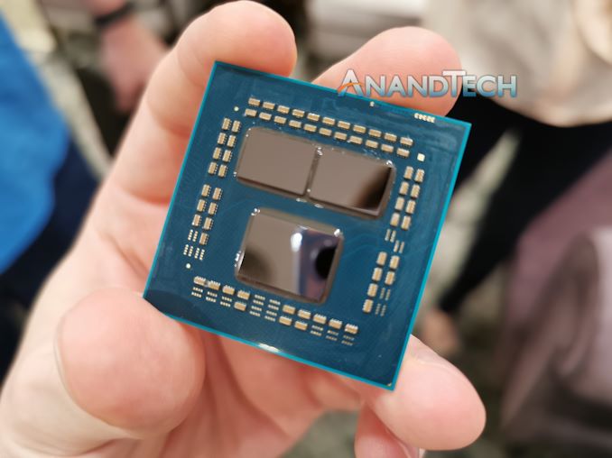
The consumer processors, known as ‘Matisse’ or Ryzen 3rd Gen or Ryzen 3000-series, will be offered with up to two chiplets for sixteen cores. AMD is launching six versions of Matisse on July 7th, from six cores to sixteen cores. The six and eight-core processors have one chiplet, while above this the parts will have two chiplets, but in all cases the IO die is the same. This means that every Zen 2 based Ryzen 3000 processor will have access to 24 PCIe 4.0 lanes and dual channel memory. Based on the announcements today, the prices will range from $199 for the Ryzen 5 3600, up to $700+ for the sixteen core (we’re waiting on final confirmation of this price).
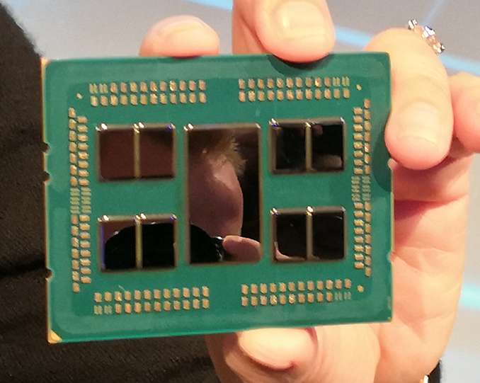
The EPYC Rome processors, built on these Zen 2 chiplets, will have up to eight of them, enabling a platform that can support up to 64 cores. As with the consumer processors, no chiplet can communicate directly with each other – each chiplet will only connect directly to the central IO die. That IO die houses links for eight memory channels, and up to 128 lanes of PCIe 4.0 connectivity.
AMD’s Roadmap
Before diving into the new product line, it is worth recapping where we currently sit in AMD’s planned roadmap.
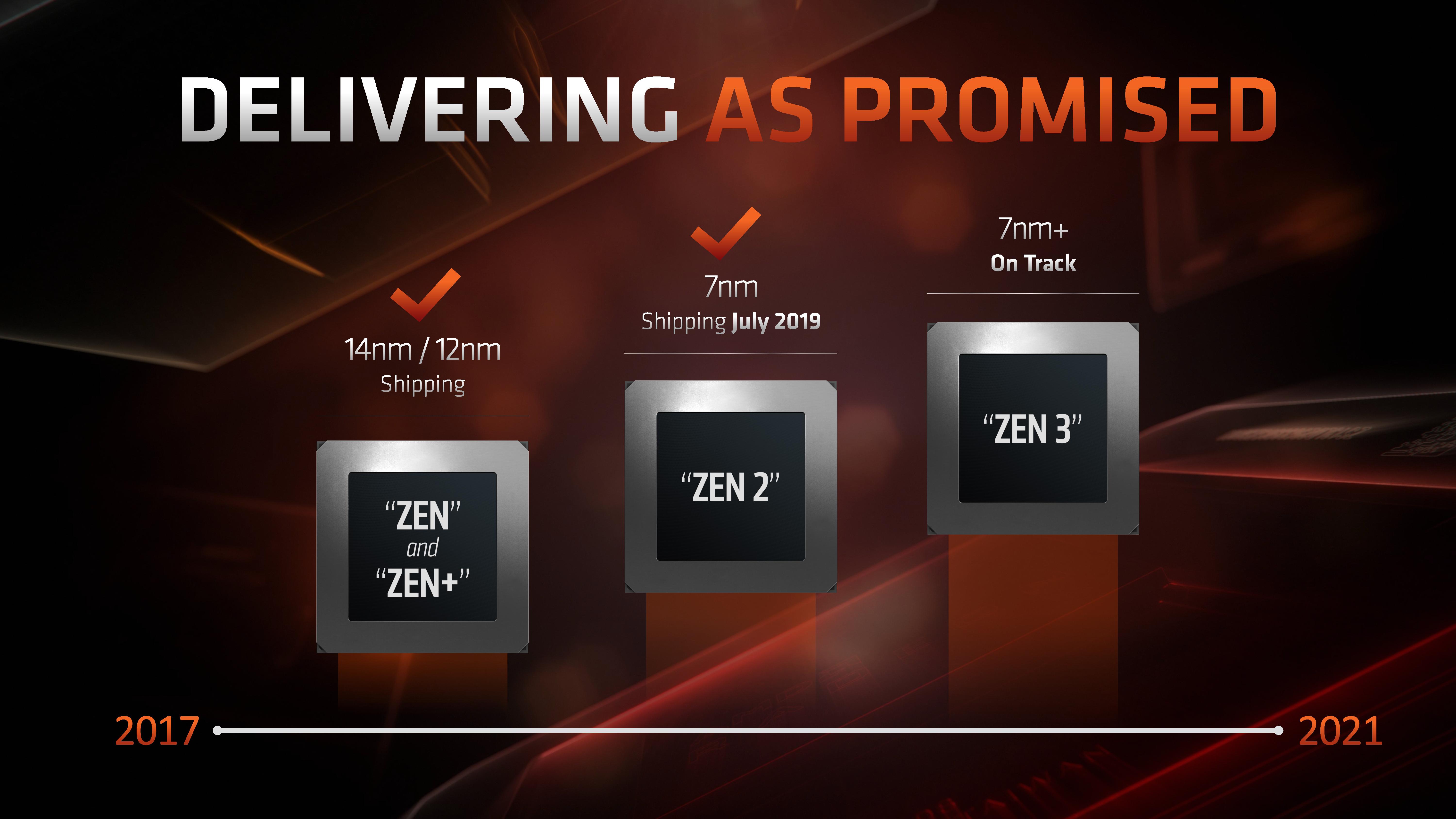
In previous roadmaps, showcasing AMD’s movement from Zen to Zen 2 and Zen 3, the company has explained that this multi-year structure will showcase Zen in 2017, Zen 2 in 2019, and Zen 3 by 2021. The cadence isn’t exactly a year, as it has depended on AMD’s design and manufacturing abilities, as well as agreements with its partners in the foundries and the current market forces.
AMD has stated that its plan for Zen 2 was to always launch on 7nm, which ended up being TSMC’s 7nm (Global Foundries wasn’t going to be ready in time for 7nm, and ultimately pulled the plug). The next generation Zen 3 is expected to align with an updated 7nm process, and at this point AMD has not made any comment about a potential ‘Zen 2+’ design in the works, although at this point we do not expect to see one.
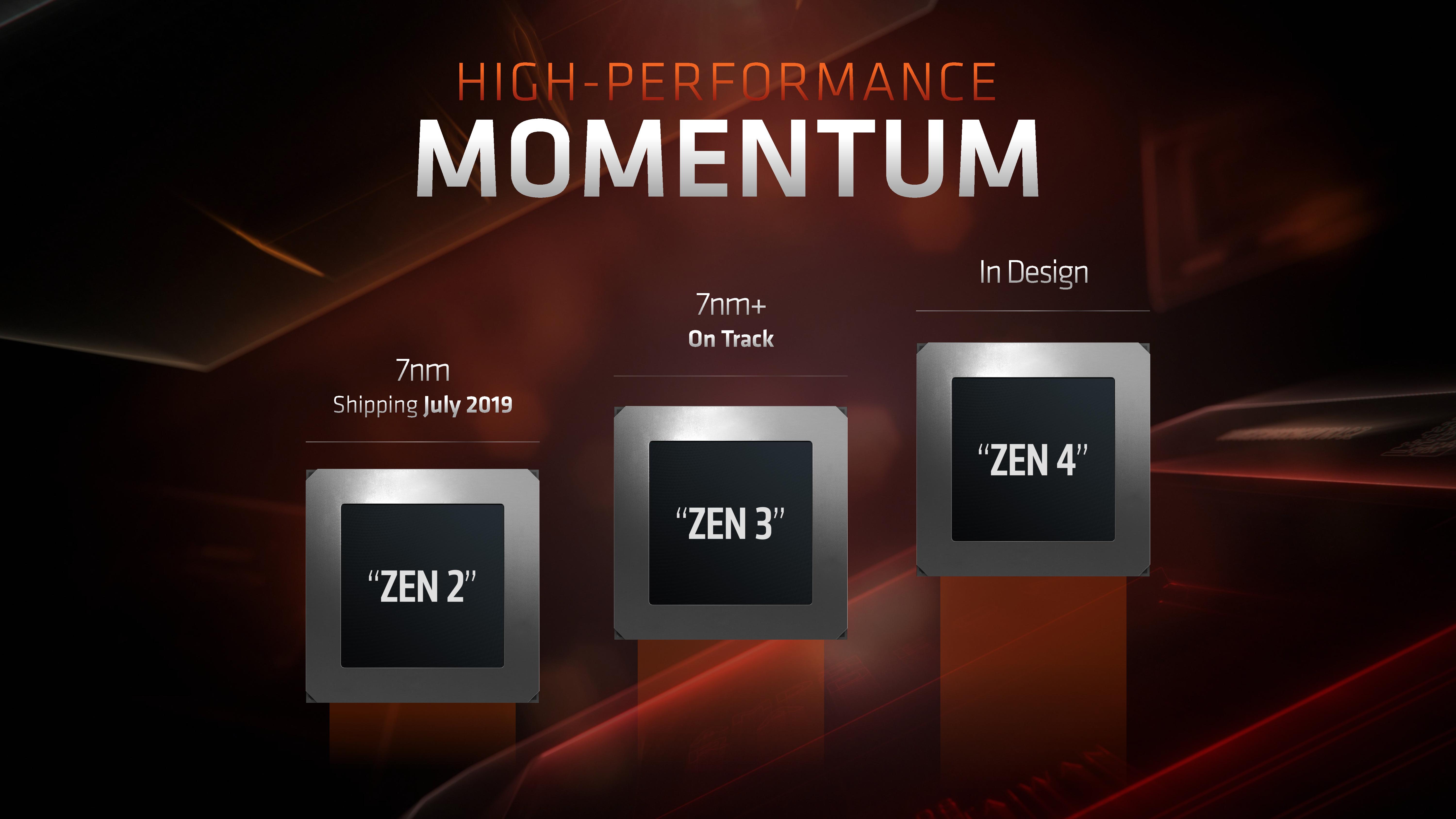
Beyond Zen 3, AMD has already stated that Zen 4 and Zen 5 are currently in various levels of their respective design stages, although the company has not committed to particular time frames or process node technologies. AMD has stated in the past that the paradigms of these platforms and processor designs are being set 3-5 years in advance, and the company states it has to make big bets every generation to ensure it can remain competitive.
For a small insight into Zen 4, in an interview with Forrest Norrod, SVP of AMD’s Enterprise, Embedded, and Semi-Custom group, at Computex, he exclusively revealed to AnandTech the code name of AMD’s Zen 4 EPYC processor: Genoa.
| AMD EPYC CPU Codenames | |||
| Gen | Year | Name | Cores |
| 1st | 2017 | Naples | 32 x Zen 1 |
| 2nd | 2019 | Rome | 64 x Zen 2 |
| 3rd | 2020 | Milan | ? x Zen 3 |
| 4th | ? | Genoa | ? x Zen 4 |
| 5th | ? | ? | ? x Zen 5 |
Forrest explained that the Zen 5 code name follows a similar pattern, but would not comment on the time frame for the Zen 4 product. Given that the Zen 3 design is expected mid-2020, that would put a Zen 4 product for late 2021/early 2022, if AMD follows its cadence. How this will play into AMD’s consumer roadmap plans is unclear at this point, and will depend on how AMD approaches its chiplet paradigm and any future adjustments to its packaging technology in order to enable further performance improvements.


216 Comments
View All Comments
Targon - Thursday, June 13, 2019 - link
The TDP figures are always a bit vague, because it is about the heat generation, not about power draw. A higher TDP on a chip with the same number of cores on the same design could indicate that it will overclock higher. Intel always sets the TDP to the base clock speed, while AMD has been more about what can be expected in normal usage. The higher the clock speed, the more power will be required, and the higher the amount of heat will be that needs to be handled by the cooler.So, if a chip has a TDP of 105W, then in theory, you should be able to get away with a cooler that can handle 105W of heat output, but if that TDP is based only on the base clock speed, you will want a better cooler to allow for turbo/boost for sustained periods.
wilsonkf - Monday, June 10, 2019 - link
We want faster memory for Zen/Zen+ because we want higher IF clock, so cutting the IF clock by half to enable higher memory freq. does not make sense. However the improved IF could move the bottleneck somewhere else.AlexDaum - Tuesday, June 11, 2019 - link
It seems like IF2 can not hit frequencies higher than about 3733MHz DDR (so 1,8GHz real frequency) for some reason, so they added the ability to scale it down to have higher memory clocks. But it is probably only worth it if you can overclock memory a lot higher than 3733, so that the IF clock gets a bit higher againXyler94 - Tuesday, June 11, 2019 - link
If I recall, IF2's clock speed is decoupled from RAM speed.Cooe - Tuesday, June 11, 2019 - link
This is wrong Xyler. Still completely connected.Xyler94 - Thursday, June 13, 2019 - link
Per this exact Article:"One of the features of IF2 is that the clock has been decoupled from the main DRAM clock. In Zen and Zen+, the IF frequency was coupled to the DRAM frequency, which led to some interesting scenarios where the memory could go a lot faster but the limitations in the IF meant that they were both limited by the lock-step nature of the clock. For Zen 2, AMD has introduced ratios to the IF2, enabling a 1:1 normal ratio or a 2:1 ratio that reduces the IF2 clock in half."
It seems it has been, but it may still benefit from faster RAM still
extide - Monday, June 17, 2019 - link
It is completely connected -- you can just pick a 1:1 or 2:1 divider now but they are absolutely still tightly coupled. YOu can't just set them independently.Cooe - Tuesday, June 11, 2019 - link
You're missing the point for >3733MHz memory overclocked where the IF switches to a 2:1 divider. It's for workloads that highly prioritize memory bandwidth over latency, NOT to try and run your sticks 24/7 at like 5GHz+ for the absolute lowest latency possible (bc even then, 3733MHz will prolly still be lower).Targon - Thursday, June 13, 2019 - link
From what I remember, up to DDR4-3733, Infinity Fabric on Ryzen 3rd generation is now at a 1:1(where previously, Infinity Fabric would run at half the DDR4 speed. You can go above that, but then the improvements are not going to be as significant. For latency, your best bet is to get 3733 or 3600 with as low a CAS rating as you can get.zodiacfml - Tuesday, June 11, 2019 - link
that 105W TDP is a sign that the 8 core is efficient at 50W or a base clock of 3.5 GHz. The AMD 7nm 8-Core Zen 2 chip has a TDP equal or less than my i3-8100.😅