Examining Intel's Ice Lake Processors: Taking a Bite of the Sunny Cove Microarchitecture
by Dr. Ian Cutress on July 30, 2019 9:30 AM EST- Posted in
- CPUs
- Intel
- 10nm
- Microarchitecture
- Ice Lake
- Project Athena
- Sunny Cove
- Gen11
Thunderbolt 3: Now on the CPU*
One of the big failures of the Thunderbolt technology since its inception has been its adoption beyond that Apple ecosystem. In order to use it, both the host and the device needed TB controllers supplied by Intel. It wasn’t until Thunderbolt 3 started to use USB Type-C, and Thunderbolt 3 having enough bandwidth to support external graphics solutions, that we started to see the number of available devices start to pick up. The issue still remains that the host and device need an expensive Intel-only controller, but the ecosystem was starting to become more receptive to its uses.
With Ice Lake, that gets another step easier.
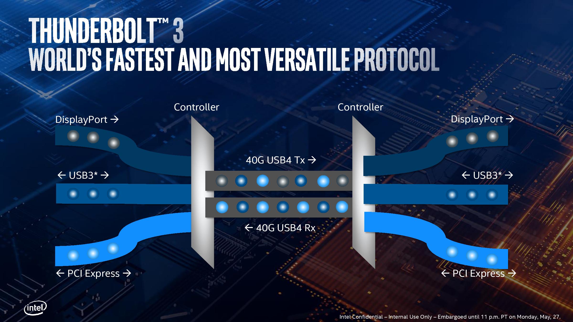
Rather than bundle TB3 support into the chipset, Intel has integrated it on the die of Ice Lake, and it takes up a sizable amount of space. Each Ice Lake CPU can support up to four TB3 ports, with each TB3 port getting a full PCIe 3.0 x4 root complex link internally for full bandwidth. (For those keeping count, it means Ice Lake technically has 32 PCIe 3.0 lanes total).
Intel has made it so each side of the CPU can support two TB3 links direct from the processor. There is still some communication back and forth with the chipset (PCH), as the Type-C ports need to have USB modes implemented. It’s worth noting that TB3 can’t be directly used out of the box, however.
Out of the four ports, it will be highly OEM dependent on how many of those will actually make it into the designs – it’s not as simple as just having the CPU in the system, but other chips (redrivers) are needed to support the USB Type-C connector. Power delivery too requires extra circuitry, which costs money. So while Intel advertises TB3 support on Ice Lake, it still needs something extra from the OEMs. Intel states that a retimer for the integrated solution is only half the size compared to the ones needed with the TB3 external chips, as well as supporting two TB3 ports per retimer, therefore halving the number of retimers needed.
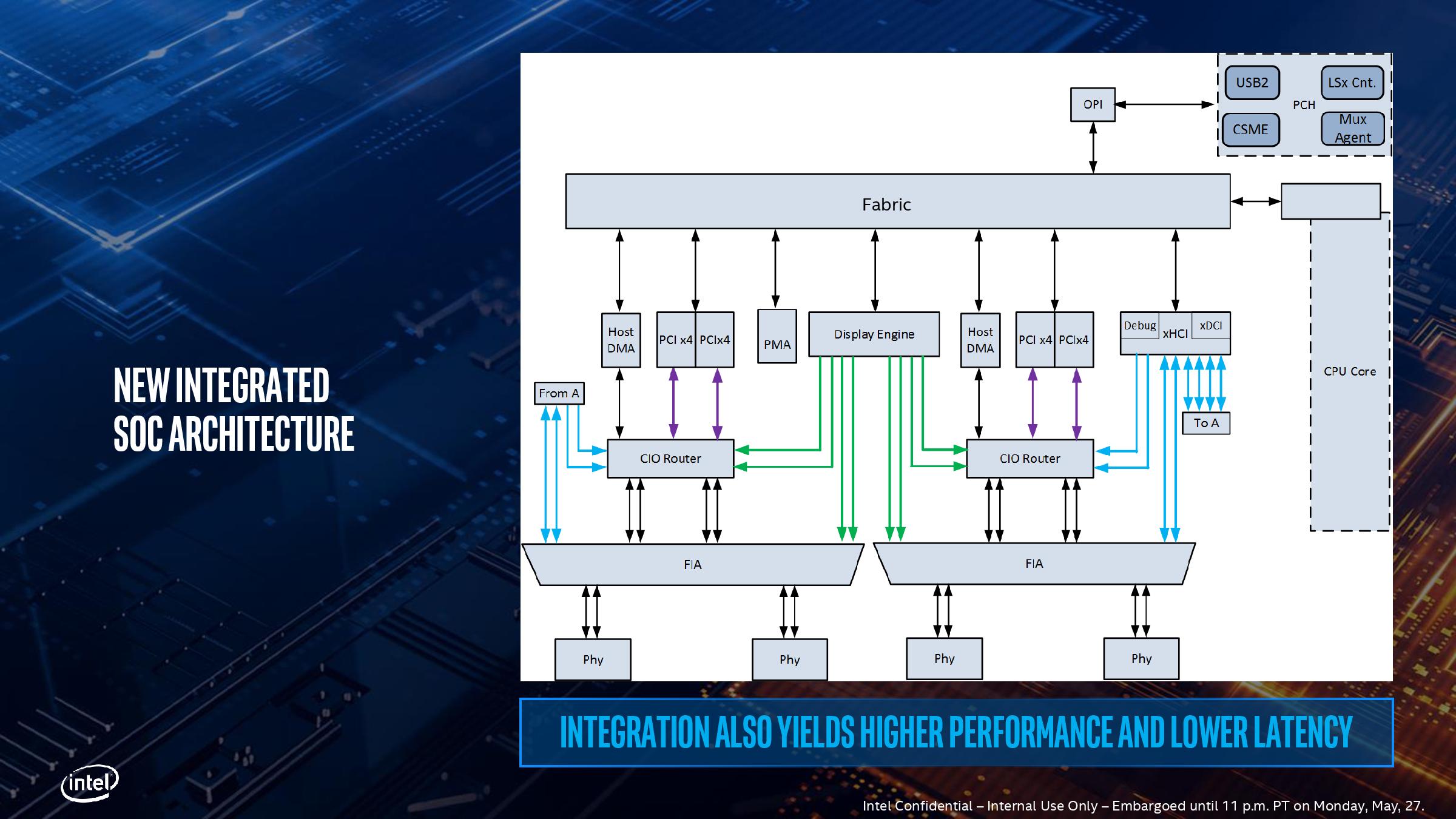
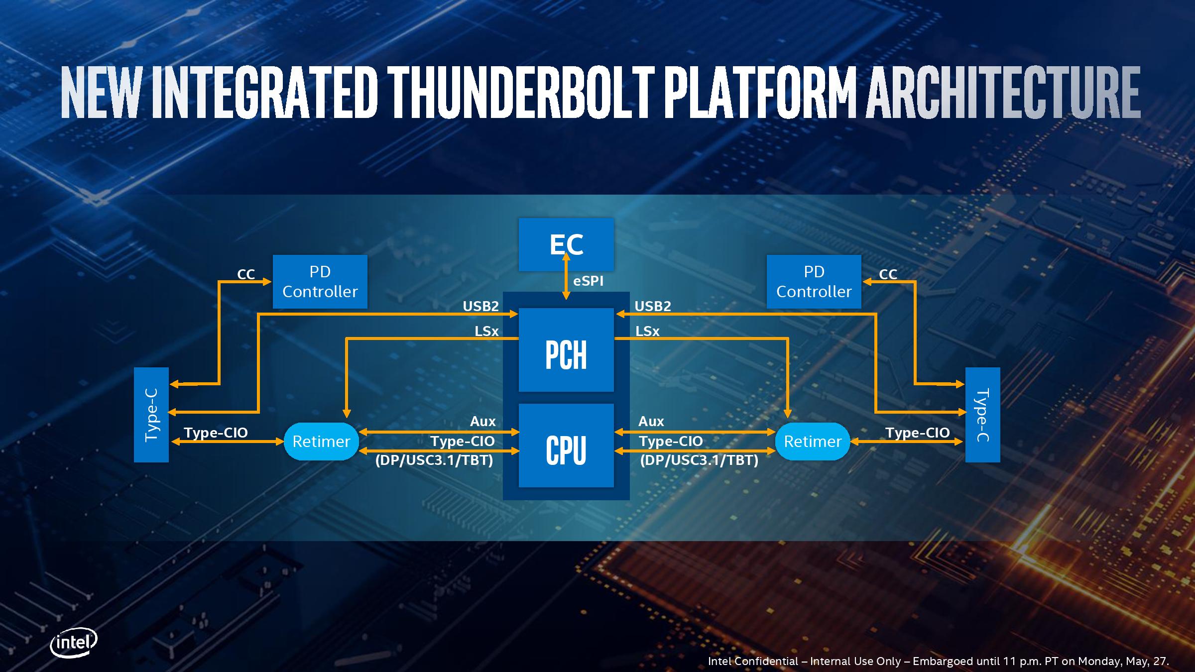
Here’s a more detailed schematic, showing the complexities of adding in TB3 into a chip, with the four PCIe x4 complexes shown moving out to each of the individual PHYs at the bottom, and connected back into the main SoC interconnect fabric. The display engine also has to control what mode the TB3 ports are in, and what signals are being sent. Wake up times for TB3 in this fashion, according to Intel, are actually slightly longer compared to a controller implementation, because the SoC is so tightly integrated. This sounds somewhat counterintuitive, given that the requisite hardware blocks are now closer together, but it all comes down to power domains – in a separate chip design, each segment has a separate domain with individual power up/down states. In an integrated SoC, Intel has unified the power domains to reduce complexity and die area, which means that more careful management is required but latency ultimately increases a little bit.
The other upside to the tightly coupled integration is that Intel stated that this method of TB3 is a lot more power efficient that current external chip implementations. However they wouldn’t comment on the exact power draw of the TB3 block on the chip as it corresponds to the full TDP of the design, especially in relation to localized thermal density (Intel was initially very confused by my question on this, ultimately saying that the power per bit was lower compared to the external chip, so overall system power was lower – they seemed more interested in discussing system power over chip power). Intel did state that the difference between an idle and a fully used link was 300 mW, which suggests that if all four links are in play, we’re looking at 1.2 W. When asked, Intel stated that there are three different power delivery domains within the TB3 block depending on the logic, that the system uses integrated voltage regulation, and the TB3 region has an internal power rail that is shared with some of the internal logic of the CPU. This has implications when it comes to time-to-wake and idle power, but Intel believes it has found a good balance.
Regarding USB4 support, Intel stated that it is in the design, and they are USB4 compliant at this point, but there might be changes and/or bugs which stop it from being completely certified further down the line. Intel said that it ultimately comes down to the device side of the specification, although they have put as much in as they were able given the time constraints of the design. They hope to be certified, but it’s not a guarantee yet.
Depending on who you speak to, this isn’t Intel’s first crack at putting TB3 into CPU silicon: the chip that Intel never wants to talk about, Cannon Lake, supposedly also had an early TB3 design built inside that never worked. But Intel is confident in its Ice Lake implementation, especially with supporting four ports. I wouldn’t be surprised if this comes to desktop when Intel releases its first generation 10nm desktop processors.
*The asterisk in the title of this page is because you still need external hardware in order to enable TB3.


107 Comments
View All Comments
Billy Tallis - Wednesday, July 31, 2019 - link
A lot of the chemicals used in wafer processing are quite nasty. A bare wafer itself is pretty harmless unless you grind it up and inhale it. Solid elemental silicon or silicon dioxide is safe to handle.repoman27 - Tuesday, July 30, 2019 - link
I understand that there are embargos which must be respected and that Anandtech does not like to trade in unsubstantiated rumors, but much of what is presented regarding packaging and power seems a bit wishy-washy.Wikichip has had photos of both sides of the Ice Lake U and Y packages posted for some time now. Furthermore, Intel's product briefs are very clear on the power for each series:
Ice Lake Y: Nominal TDP 9 W, cTDP Down 8 W on Core i3 only, cTDP Up 12 W but N/A on Core i3,
Ice Lake U: Nominal TDP 15 W, cTDP Down 12 W (13 W for some UHD parts), cTDP Up 25 W
AFAIK, no 28 W Ice Lake-U parts have been announced by Intel yet, but they most likely are in the works.
And you can cite whatever reasons you care to, but by all reports Intel was initially targeting a 5.2 W TDP for Ice Lake-Y 4+2, and that entire platform has been solidly shifted into the 8-12 W range.
Also, it should be noted that the 14nm 300 Series chipsets that Intel has been shipping for some time now are all Cannon Point, which was originally designed to complement Cannon Lake, and are almost identical in terms of capabilities to the 400 Series. And the particular designation for the Ice Lake PCH-LP according to Intel is "495 Series".
James5mith - Tuesday, July 30, 2019 - link
Ian,You either have your graph or your paragraph about the store/load performance increases reversed.
Graph says 72 -> 128 stores, 56 -> 72 loads. The paragraph below it says 72-128 loads, 56-> 72 stores.
ksec - Tuesday, July 30, 2019 - link
While I do enjoy and mostly want to read Dr Ian Cutress article, I seriously don't want to read Intel's marketing hype. Action and Results speaks louder than Powerpoint slides. Ship it, let Anandtech test it. And we make an opinion on it.Targon - Tuesday, July 30, 2019 - link
The Ryzen 7 3700U is a Zen+ part on 12nm, without the big IPC plus clock speed improvements seen with the desktop CPUs. As a result, Intel is doing a comparison against the previous generation products for laptops.In laptops, getting max turbo or boost for more than one second is rare. Yea, Intel can put a laptop chip on a board on a bench without any enclosure to show the chip, but real world speeds will be quite a bit lower. That is true for both AMD as well as Intel, and it is up to the OEMs to come up with a design to keep the chips cool enough to run faster than the competition.
AMD knows what is going on, so if I am correct, AMD will move up the release of the next generation of laptop chips to November. If AMD does the right thing, AMD will call the new chips the 3250U, 3400U, 3600U, and 3800U to bring consistency with desktop naming conventions. These new chips would be 7nm with either Vega or Navi, for an APU it is less important than going 7nm for both.
Drumsticks - Tuesday, July 30, 2019 - link
Keep in mind, the only comparison they did with Ryzen (I think) was Graphics, not CPU. I'd imagine the Icelake chips have a solid CPU lead against quad core Ryzen based on Zen/Zen+. Zen 2 will certainly help close that gap, but it should still be roughly 15-20% behind Icelake in IPC, and I certainly won't be ahead that much on frequency.Fulljack - Wednesday, July 31, 2019 - link
I think in Q4 19 they'd release Ryzen 4000 series (based on Zen 2) and call it day, like last year or two year ago.they'll be 4300U, 4500U, and 4700U for U-series and 4350H, 4550H, and 4750H for high-performance part with integrated graphics based on Navi.
but since Zen 2 has 8 cores now on each CCX, they'd probably also sell 6-core and 8-core part, but I don't know if they'll release it on U-series, though.
Apple Worshipper - Tuesday, July 30, 2019 - link
Thanks Ian ! So how does Ice Lake purportedly stand next to Apple’s A12x in iPad Pro based on the Spec scores ?PeachNCream - Tuesday, July 30, 2019 - link
More importantly, how does Ice Lake taste?HStewart - Tuesday, July 30, 2019 - link
I have seen anything that was successfully comparing x86 based cpus with AEM based cpusBut one things - that makes all this MacBook ARM stuff meaningless to me is one sheer fact - Apple has yet to release development tools for iOS on actual iOS. It might be Apple trying force Macs for development but Apples own development tools don't run on iOS