Examining Intel's Ice Lake Processors: Taking a Bite of the Sunny Cove Microarchitecture
by Dr. Ian Cutress on July 30, 2019 9:30 AM EST- Posted in
- CPUs
- Intel
- 10nm
- Microarchitecture
- Ice Lake
- Project Athena
- Sunny Cove
- Gen11
Gen11 Graphics: Competing for 1080p Gaming
The new message from Intel is that it is driving to deliver deep gaming experiences with its technology, and the nod to the future is specifically what it wants to do with its graphics technology. Until the company is ready with its Xe designs for 2020 and beyond, it wants to start to lead the way with better integrated designs. That starts with Ice Lake, where the most powerful version of Ice Lake will offer over 1TF of compute performance, support higher resolution HEVC, better display pipes, an enhanced rasterizer, and support for Adaptive Sync.
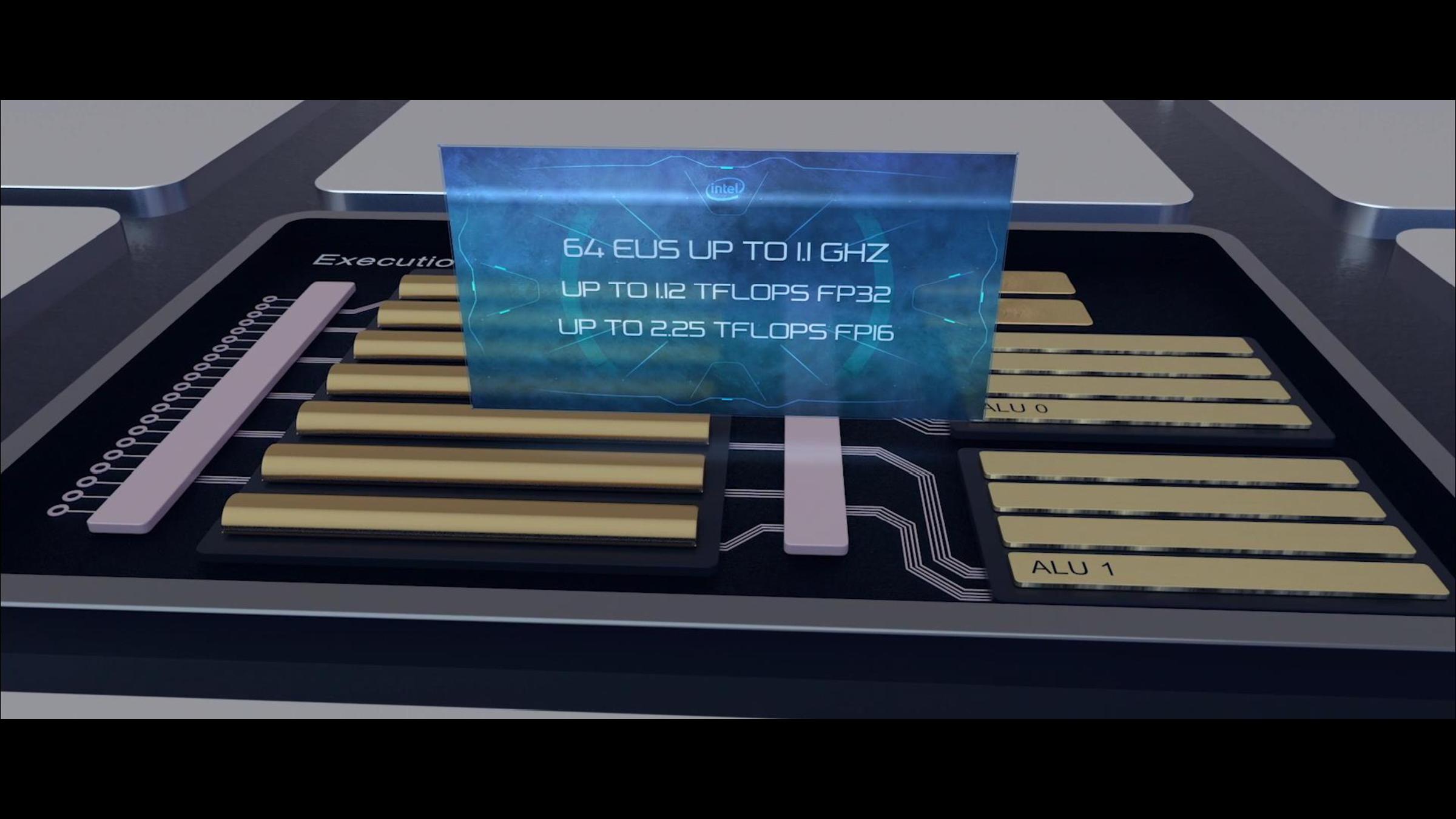
The key words in that last sentence were ‘the most powerful version’. Because Intel hasn’t really spoken about its product stack yet, the company has been leading with its most powerful Iris Plus designs. We assume this means 28W? That means its high-end performance products, in the best designs, with the fastest memory. Compared to the standard Gen9 implementation of 24 execution units at 1150 MHz turbo, the best Ice Lake Gen11 design will deliver 64 execution units up to a 1100 MHz frequency, good for 1.15 TF of FP32 performance, or 2.30 TF of FP16 performance. Intel promise up to 1.8x better frame rates in games with the best Ice Lake compared to an average 8th Gen Core (Kaby Lake) Gen9 implementation. Intel doesn’t compare the results to a hypothetical Cannon Lake Gen10 implementation.
Intel hasn’t stated how many graphics configurations it will offer, but there would appear to be several given what information has leaked out already. The high-end design with 64 execution units will be called Iris Plus, but there will be a ‘UHD’ version for mid-range and low-end parts, however Intel has not stated how many execution units these parts will have. We suspect that standard dividers will be in play, with 24/32/48 EU designs possible as different parts of the GPU are fused off. There may be some potential for increased frequency in these designs, reducing latency, but ultimately reduced performance over the top design.
It should be noted that Intel is promoting the top model as being suitable for 1080p low-to-mid gaming, which would imply that models with fewer execution units may struggle to hit those highs with different EU counts. Until Intel gives us a full and proper product list, it is hard to tell at this point.
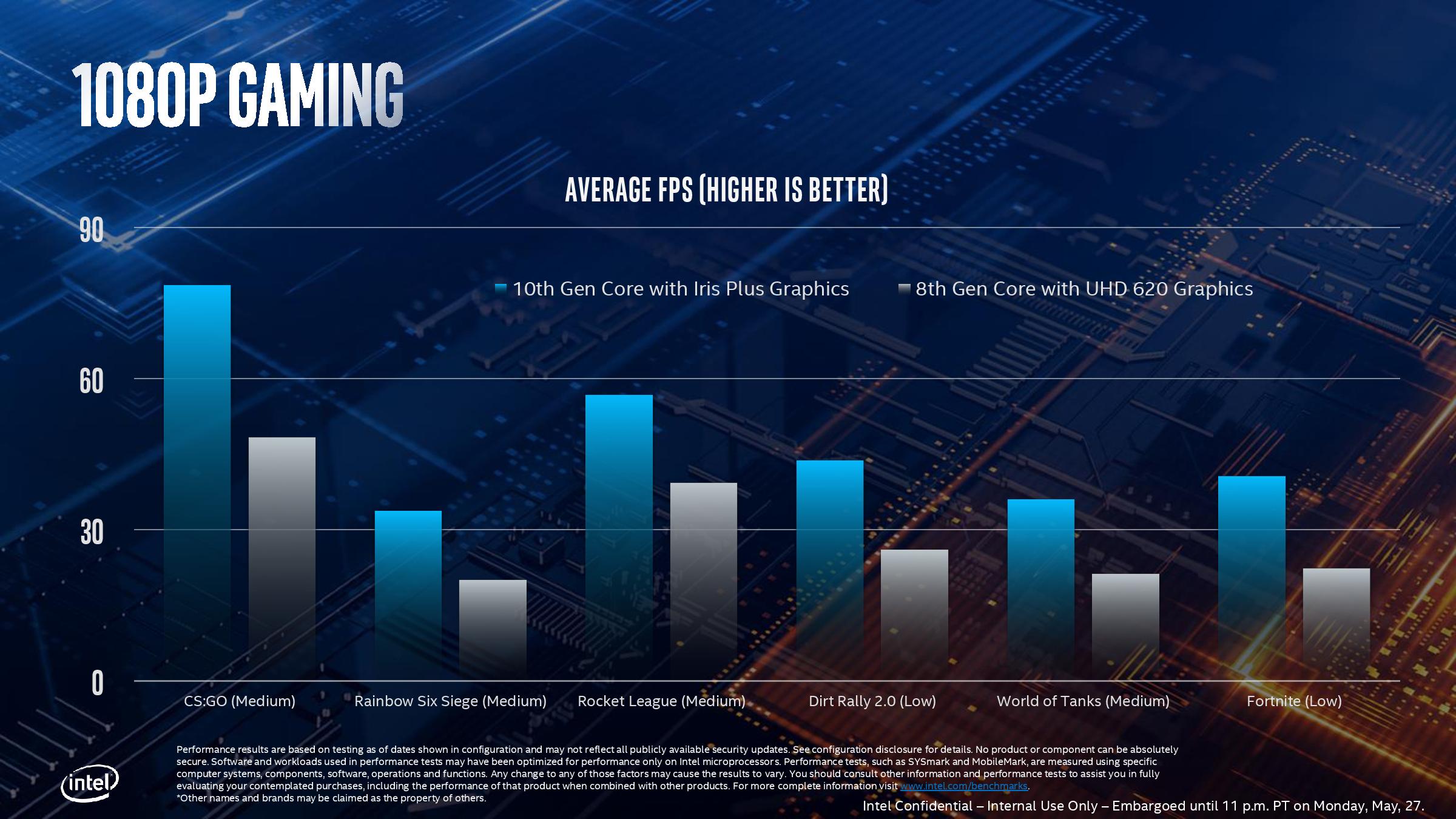
This slide, for example, shows where Intel expects its highest Ice Lake implementation to perform compared to the standard 8th Gen solution. As part of Computex, Intel also showed off some different data:
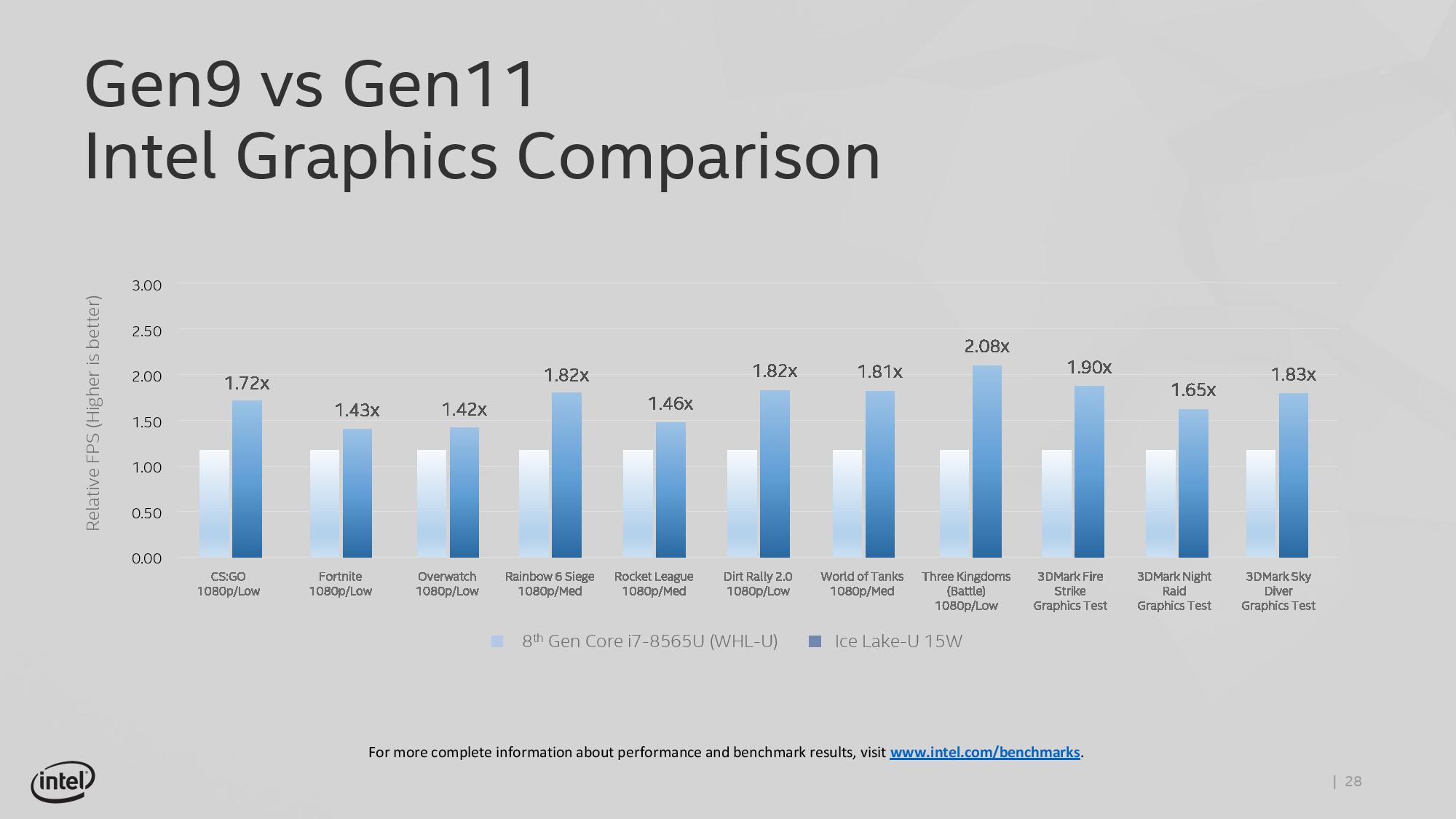
This graph shows relative FPS, rather than actual FPS, so it’s hard to see if certain games are just hitting 30 FPS in the highest mode. The results here are a function of the combination of increased EU count but also memory bandwidth.
Features for All
There are a number of features that all of the Gen11 graphics implementations will get, regardless of its number of execution units.
For its fixed function units, Gen11 supports two HEVC 10-bit encode pipelines, either two 4K60 4:4:4 streams simultaneously or one 8K30 4:2:2 stream using both pipelines at once. On display pipes, Gen11 has access to three 4K pipes split between DP1.4 HBR3 and HDMI 2.0b. There is also support for 2x 5K60 or 1x 4K120 with a 10-bit color depth.
The rasterizer gets an upgrade, and will now do 16 pixels per clock or 32 bilinear filtered texels per clock. Intel also gives some insight into the cache arrangements, with the execution units having their own 3 MiB of L3 cache and 0.5 MiB of shared local memory.
Intel recommends that to get the best out of the graphics, it should be paired with LPDDR4X-3733 memory in order to extract a healthy 50-60 GB/s bandwidth, and we should expect a number of Project Athena approved designs do just that. However, at the lower end of Ice Lake devices, we might see single channel DDR4 designs take over due to costs, which might limit performance. As always for integrated graphics, memory bandwidth is often a major bottleneck in performance. Back when Intel had eDRAM enabled Crystalwell designs, those chips were good for 50 GB/s bidirectional bandwidth, and we are almost at that stage with DRAM bandwidth designs now. It should be noted that there are tradeoffs with memory support: LPDDR4/X supports 4x 32b channels up to 32 GB with super low power consumption modes, but if users want more capacity, they’ll have to look to DDR4-3200 with 2x 64b channels up to 64 GB, but lose some performance and power savings.
Variable Rate Shading
A feature being implemented in Gen11 is Variable Rate Shading. VRS is a game-dependent technology that allows the GPU adjust the shading performance of the scene render based on what areas are important. All games currently do shading on a per-pixel basis, meaning that each pixel has a full calculation and that data is transferred to the final image. With VRS, shading is calculated over several pixels at once – essentially doing pixel shading in a coarser, lower-resolution manner – to save post-processing time by using averaged data.
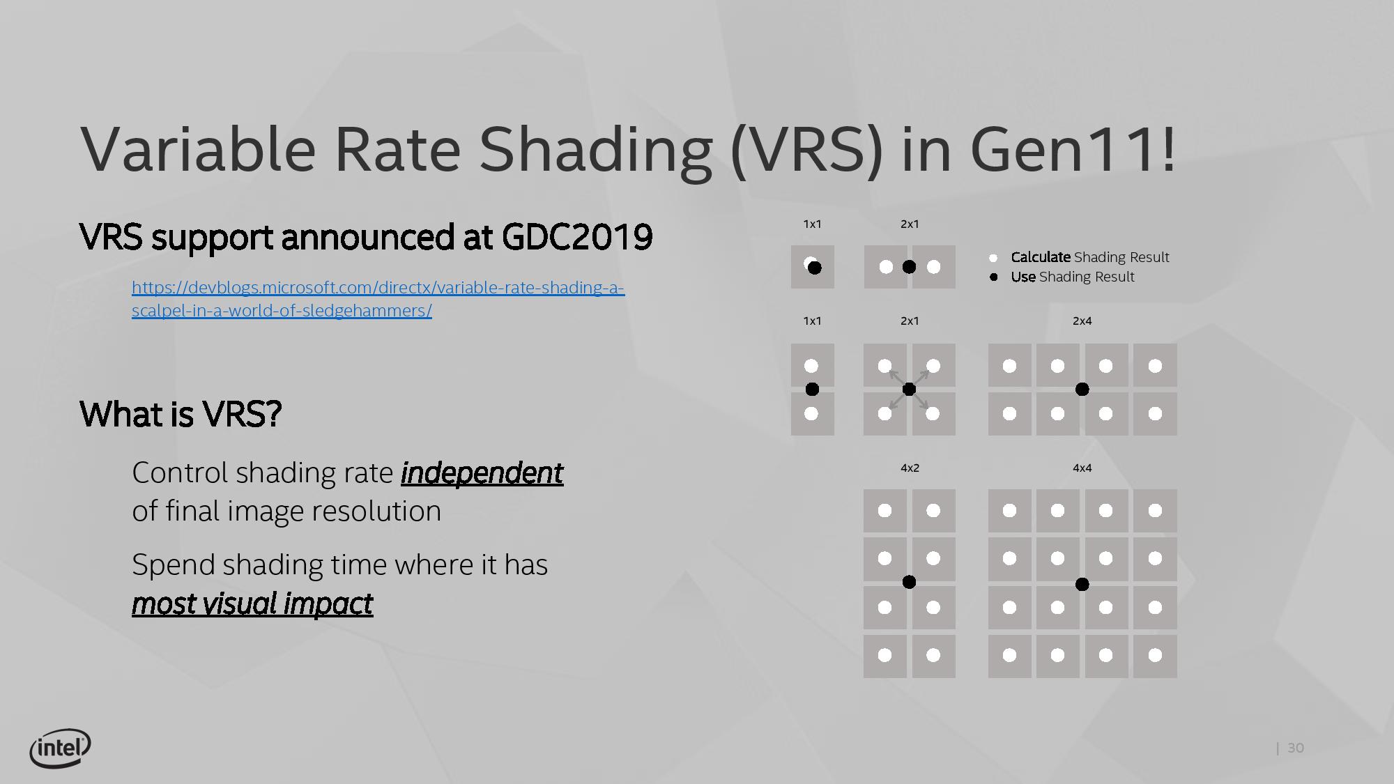
The idea is that using this method can reduce some of the load on the execution units, ultimately increasing the frame rate. The size of that combination of pixels can be adjusted on a per-frame basis as well, allowing the game to take advantage of processing budget where it exists, or pull back to a point where performance is needed. Ultimately Intel believes that any image quality loss is not noticeable, especially for the performance impact they expect it to provide. Intel states that this technology is useful for areas such as lighting adjustments, partially obscured objects (by fog/clouds), and areas that undergo blur, or foveated rendering – basically any area where clarity isn’t explicitly required to begin with.
The only issue here though is an ecosystem one – it requires the game developer support. Intel is already working with Epic to add it to the Unreal Engine, and Intel has worked with developers to enable support in titles such as Civilization 6. The difference in performance, according to Intel, can be up to a 30% FPS increase in a best-case scenario. NVIDIA already supports VRS through dedicated hardware, whereas AMD’s current solutions are best described as a more limited shader-based approximation.


107 Comments
View All Comments
Billy Tallis - Wednesday, July 31, 2019 - link
A lot of the chemicals used in wafer processing are quite nasty. A bare wafer itself is pretty harmless unless you grind it up and inhale it. Solid elemental silicon or silicon dioxide is safe to handle.repoman27 - Tuesday, July 30, 2019 - link
I understand that there are embargos which must be respected and that Anandtech does not like to trade in unsubstantiated rumors, but much of what is presented regarding packaging and power seems a bit wishy-washy.Wikichip has had photos of both sides of the Ice Lake U and Y packages posted for some time now. Furthermore, Intel's product briefs are very clear on the power for each series:
Ice Lake Y: Nominal TDP 9 W, cTDP Down 8 W on Core i3 only, cTDP Up 12 W but N/A on Core i3,
Ice Lake U: Nominal TDP 15 W, cTDP Down 12 W (13 W for some UHD parts), cTDP Up 25 W
AFAIK, no 28 W Ice Lake-U parts have been announced by Intel yet, but they most likely are in the works.
And you can cite whatever reasons you care to, but by all reports Intel was initially targeting a 5.2 W TDP for Ice Lake-Y 4+2, and that entire platform has been solidly shifted into the 8-12 W range.
Also, it should be noted that the 14nm 300 Series chipsets that Intel has been shipping for some time now are all Cannon Point, which was originally designed to complement Cannon Lake, and are almost identical in terms of capabilities to the 400 Series. And the particular designation for the Ice Lake PCH-LP according to Intel is "495 Series".
James5mith - Tuesday, July 30, 2019 - link
Ian,You either have your graph or your paragraph about the store/load performance increases reversed.
Graph says 72 -> 128 stores, 56 -> 72 loads. The paragraph below it says 72-128 loads, 56-> 72 stores.
ksec - Tuesday, July 30, 2019 - link
While I do enjoy and mostly want to read Dr Ian Cutress article, I seriously don't want to read Intel's marketing hype. Action and Results speaks louder than Powerpoint slides. Ship it, let Anandtech test it. And we make an opinion on it.Targon - Tuesday, July 30, 2019 - link
The Ryzen 7 3700U is a Zen+ part on 12nm, without the big IPC plus clock speed improvements seen with the desktop CPUs. As a result, Intel is doing a comparison against the previous generation products for laptops.In laptops, getting max turbo or boost for more than one second is rare. Yea, Intel can put a laptop chip on a board on a bench without any enclosure to show the chip, but real world speeds will be quite a bit lower. That is true for both AMD as well as Intel, and it is up to the OEMs to come up with a design to keep the chips cool enough to run faster than the competition.
AMD knows what is going on, so if I am correct, AMD will move up the release of the next generation of laptop chips to November. If AMD does the right thing, AMD will call the new chips the 3250U, 3400U, 3600U, and 3800U to bring consistency with desktop naming conventions. These new chips would be 7nm with either Vega or Navi, for an APU it is less important than going 7nm for both.
Drumsticks - Tuesday, July 30, 2019 - link
Keep in mind, the only comparison they did with Ryzen (I think) was Graphics, not CPU. I'd imagine the Icelake chips have a solid CPU lead against quad core Ryzen based on Zen/Zen+. Zen 2 will certainly help close that gap, but it should still be roughly 15-20% behind Icelake in IPC, and I certainly won't be ahead that much on frequency.Fulljack - Wednesday, July 31, 2019 - link
I think in Q4 19 they'd release Ryzen 4000 series (based on Zen 2) and call it day, like last year or two year ago.they'll be 4300U, 4500U, and 4700U for U-series and 4350H, 4550H, and 4750H for high-performance part with integrated graphics based on Navi.
but since Zen 2 has 8 cores now on each CCX, they'd probably also sell 6-core and 8-core part, but I don't know if they'll release it on U-series, though.
Apple Worshipper - Tuesday, July 30, 2019 - link
Thanks Ian ! So how does Ice Lake purportedly stand next to Apple’s A12x in iPad Pro based on the Spec scores ?PeachNCream - Tuesday, July 30, 2019 - link
More importantly, how does Ice Lake taste?HStewart - Tuesday, July 30, 2019 - link
I have seen anything that was successfully comparing x86 based cpus with AEM based cpusBut one things - that makes all this MacBook ARM stuff meaningless to me is one sheer fact - Apple has yet to release development tools for iOS on actual iOS. It might be Apple trying force Macs for development but Apples own development tools don't run on iOS