Examining Intel's Ice Lake Processors: Taking a Bite of the Sunny Cove Microarchitecture
by Dr. Ian Cutress on July 30, 2019 9:30 AM EST- Posted in
- CPUs
- Intel
- 10nm
- Microarchitecture
- Ice Lake
- Project Athena
- Sunny Cove
- Gen11
Combining 10nm CPU + 14nm Chipset
As with Intel’s previous low-power (sub 28W) mobile designs, the company will be combining the CPU and the chipset onto a single package. This typically helps in enabling a smaller motherboard design for thin and light systems that might want to dedicate that area to additional battery, or simply save the footprint altogether. The flip side is that there are more pin-outs, and the board design has to be suitable for the increased signal traces, but this is nothing new. For Ice Lake-U, Intel has stated that the CPU, which is being built on their second-generation 10nm "10+" process, will be paired with a new generation ‘14nm class’ chipset.
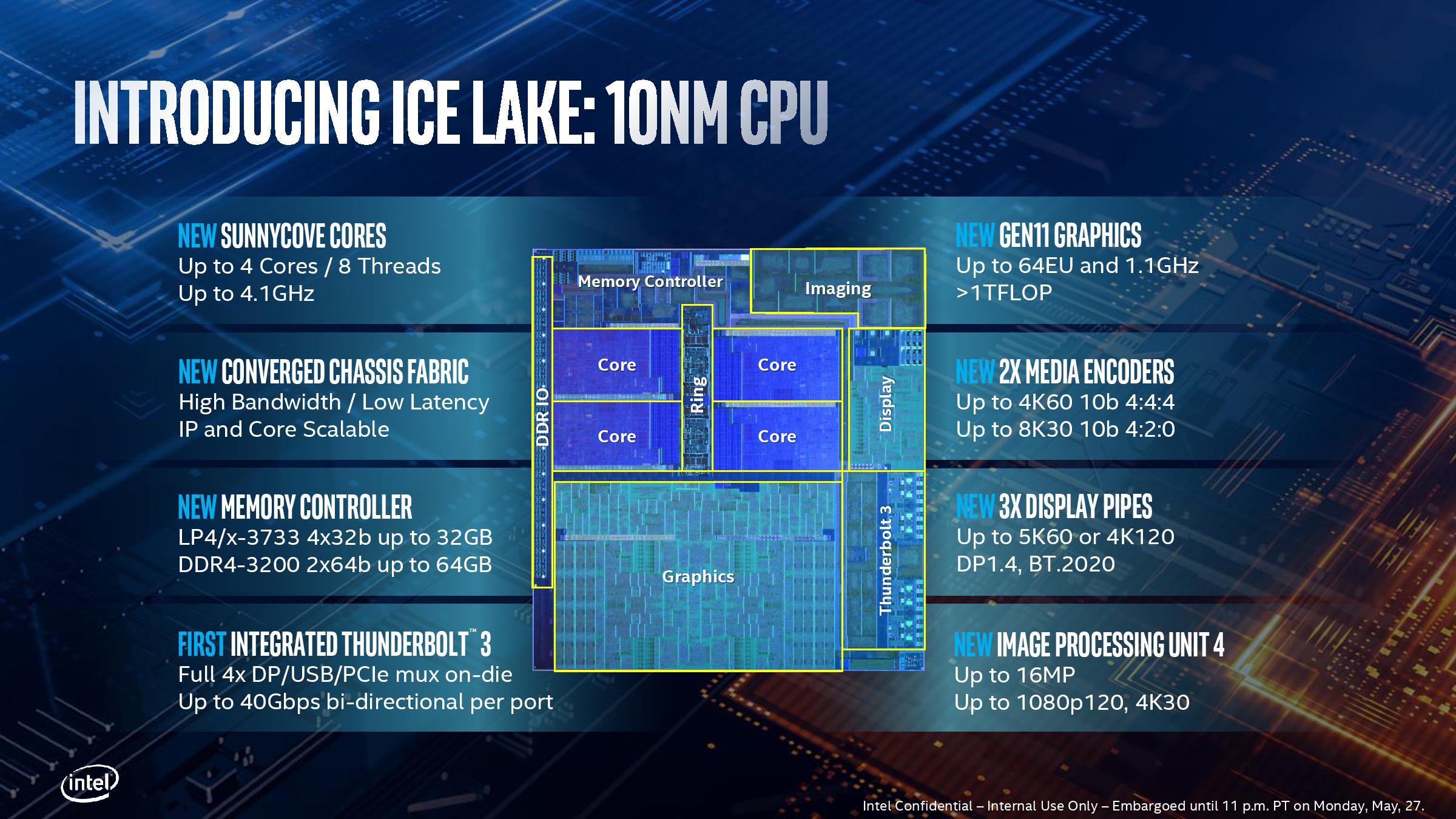
As stated on the previous page, the CPU will offer up to four cores, eight threads, go up to 4.1 GHz, provide integrated TB3 (more on that later), and a vast improvement to the graphics capabilities (also more on that later).
One of the big updates to the design will be enabling support for both DDR4 and LPDDR4/LPDDR4X on a single memory controller. Up until this point, only Intel’s latest Atom designs had LPDDR4 enabled, so this is a welcome addition to the main high-performance product line. In this instance Intel will support LPDDR4/X with up to four 32-bit channels at 3733 MT/s for 32 GB, or if a user needs more capacity, up to 64GB of DDR4-3200 with two 64-bit channels. The LPDDR4/X implementation will allow for lower idle power states, saving power and battery life when the memory is not in use, however it does this in exchange for maximum capacity. It’s an interesting tradeoff for sure. The peak power consumption of both modes in an equally populated system, given the respective frequency difference, should be similar.
One element that Intel hasn’t talked about is its ‘new converged chassis fabric’, which we believe to be a scalable power and environment control fabric that connects between chips in order to both transfer data but also to manage how and where power is applied within a system. The fact that Intel calls this ‘IP and Core scalable’ suggests that if vendors want to add additional supported chips to the system, say for example a future Intel AI chip, that might be possible and it could be controlled through this fabric. It will be interesting to see if Intel divulges any more of this information.
Not mentioned in this slide are the new performance enhancements, such as AVX-512 and other new instructions, which we’ll cover in detail a bit later.
The connection to the chipset is through a DMI 3.0 x4 link, as with current generations of Intel products.
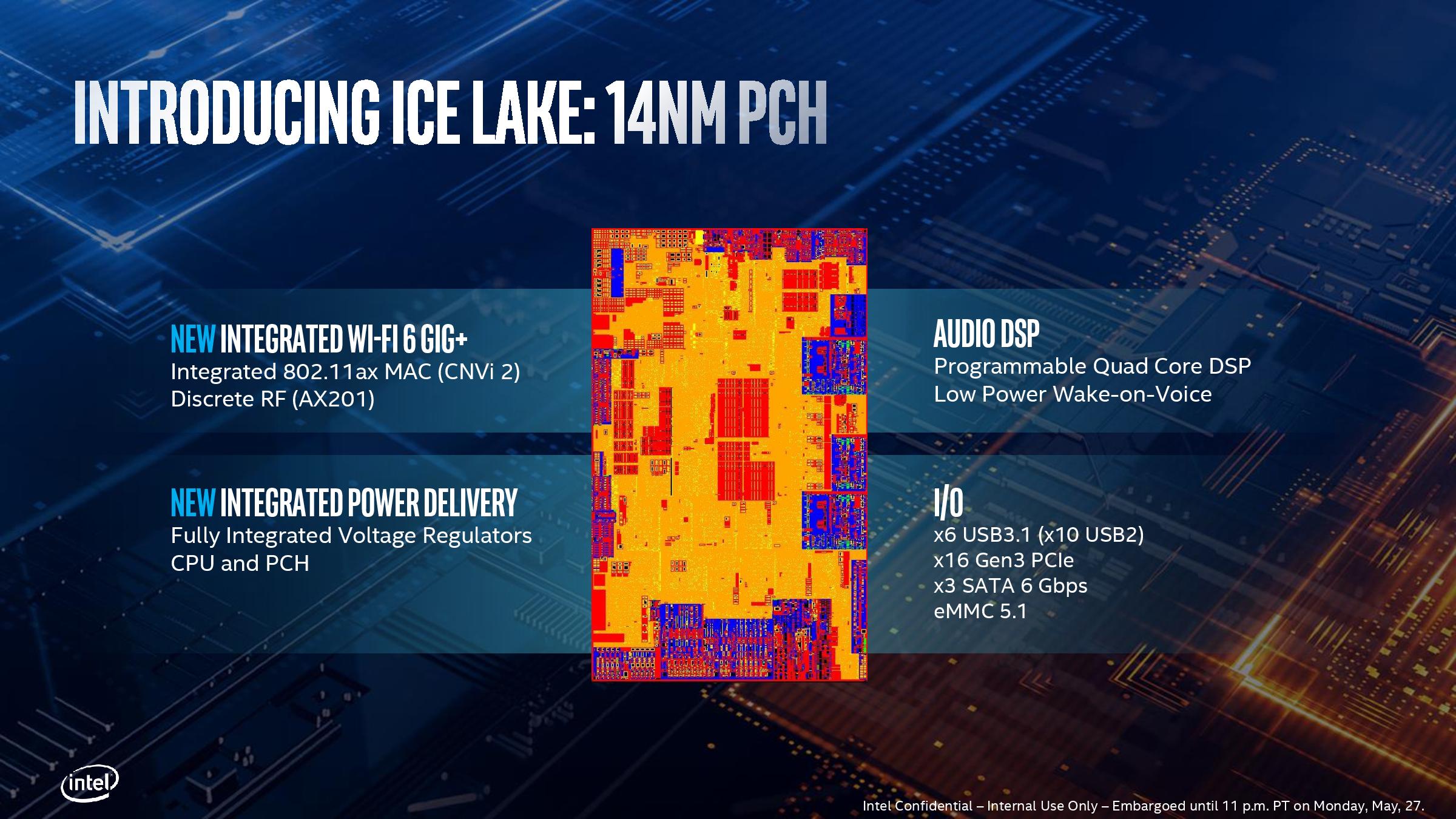
The new ‘14nm class’ chipset is also an update from Intel’s 8th Gen Core mobile processors. It does not yet have a series designation, but given the updates, this is likely to be a member of the 400-series chipset line.
With the new chipset, Intel has updated the proprietary CNVi protocol on the die to support CNVi 2, which is found on the latest Wi-Fi 6 Intel-Only RF modules, such as AX201. This update to a second generation implementation is likely to be for throughput reasons, given the increased bandwidth that Wi-Fi 6 provides over Wi-Fi 5.
Intel also promotes better integrated power delivery on the chipset, meaning that the PCH can share the same power rail as the CPU, reducing the number of on-board components inside the mobile system. This should reduce cost, and hopefully the thermal density of the power delivery onboard the chip doesn’t have a negative effect. Also on the power side, Intel states that the audio DSP on the chipset has also been improved for lower power operation.
On the IO side of the chipset, Ice Lake will support up to six ports of USB 3.1 (which is now USB 3.2 Gen 1 at 5 Gbps), or 10 USB 2.0 ports, or a mix. There are also 16 HSIO lanes which are broadly presented as PCIe 3.0, although given previous HSIO models it is likely that certain combinations of ports will be required for specific features. However this should afford at least two, if not three, potential PCIe 3.0 x4 NVMe drives in these systems. For SATA, there is access to three direct ports, but there is also an eMMC 5.1 link. Intel does not state if UFS is supported for super-small form factor systems.
Ice Lake is not Intel’s first crack at 10nm
We documented the history of Intel’s 10nm process with our review of the first 10nm CPU to come from the company. Our Core i3-8121U analysis of the Cannon Lake design is one Intel would rather forget – the manufacturing process didn’t yield, the frequency wasn’t there, the power consumption was too high, and the graphics were completely fused off. But hey, Intel still shipped it to customers by the end of 2017, and it found its way into some Chinese educational notebooks, and some NUCs, eventually, satisfying promises made to shareholders.

Fast forward almost 18 months, and we’re about to see Intel’s second take on 10nm with Ice Lake. Under Intel’s nomenclature, Ice Lake is technically being built with the ‘10+’ process, which is meant to be an improved version of the 10nm used in Cannon Lake. The fact that parts of the CPU are now working means that it earns that plus. Intel pointed to an extra metal layer (going from 12 to 13) in the manufacturing has helped with power delivery and frequency, and new transistor library designs and MIM caps have helped with voltages. Intel is also using a thin magnetic inductor array, and a recess in motherboard design for reduced package z-height.
As for Intel’s future, the company has stated at events that it is now developing future process nodes with these ‘BKM’ updates built into the lifecycle of the process node, such as 10+ and 10++ as part of the family of 10nm processes, and then beyond to 7nm with 7, 7+, and 7++ over the next few years. It’s worth noting that while Intel has officially shipped a first generation 10nm product, is promoting Ice Lake as a ‘10+’ second generation 10nm product, and has specified a number of 10nm class products up and down its product portfolio, we are still waiting on an official presentation about how Intel’s 10nm process works in a formal setting, rather than bits and pieces from events like ISSCC and IEDM. What we have pieced together from those events is likely out of date for 10+, however we do know that for 10nm Intel has three different libraries based on performance, each with different transistor densities: from 67 million transistors / mm2 for ultra-high performance, to 101 million transistors / mm2 for high-density logic. You can read more about it here.


107 Comments
View All Comments
Billy Tallis - Wednesday, July 31, 2019 - link
A lot of the chemicals used in wafer processing are quite nasty. A bare wafer itself is pretty harmless unless you grind it up and inhale it. Solid elemental silicon or silicon dioxide is safe to handle.repoman27 - Tuesday, July 30, 2019 - link
I understand that there are embargos which must be respected and that Anandtech does not like to trade in unsubstantiated rumors, but much of what is presented regarding packaging and power seems a bit wishy-washy.Wikichip has had photos of both sides of the Ice Lake U and Y packages posted for some time now. Furthermore, Intel's product briefs are very clear on the power for each series:
Ice Lake Y: Nominal TDP 9 W, cTDP Down 8 W on Core i3 only, cTDP Up 12 W but N/A on Core i3,
Ice Lake U: Nominal TDP 15 W, cTDP Down 12 W (13 W for some UHD parts), cTDP Up 25 W
AFAIK, no 28 W Ice Lake-U parts have been announced by Intel yet, but they most likely are in the works.
And you can cite whatever reasons you care to, but by all reports Intel was initially targeting a 5.2 W TDP for Ice Lake-Y 4+2, and that entire platform has been solidly shifted into the 8-12 W range.
Also, it should be noted that the 14nm 300 Series chipsets that Intel has been shipping for some time now are all Cannon Point, which was originally designed to complement Cannon Lake, and are almost identical in terms of capabilities to the 400 Series. And the particular designation for the Ice Lake PCH-LP according to Intel is "495 Series".
James5mith - Tuesday, July 30, 2019 - link
Ian,You either have your graph or your paragraph about the store/load performance increases reversed.
Graph says 72 -> 128 stores, 56 -> 72 loads. The paragraph below it says 72-128 loads, 56-> 72 stores.
ksec - Tuesday, July 30, 2019 - link
While I do enjoy and mostly want to read Dr Ian Cutress article, I seriously don't want to read Intel's marketing hype. Action and Results speaks louder than Powerpoint slides. Ship it, let Anandtech test it. And we make an opinion on it.Targon - Tuesday, July 30, 2019 - link
The Ryzen 7 3700U is a Zen+ part on 12nm, without the big IPC plus clock speed improvements seen with the desktop CPUs. As a result, Intel is doing a comparison against the previous generation products for laptops.In laptops, getting max turbo or boost for more than one second is rare. Yea, Intel can put a laptop chip on a board on a bench without any enclosure to show the chip, but real world speeds will be quite a bit lower. That is true for both AMD as well as Intel, and it is up to the OEMs to come up with a design to keep the chips cool enough to run faster than the competition.
AMD knows what is going on, so if I am correct, AMD will move up the release of the next generation of laptop chips to November. If AMD does the right thing, AMD will call the new chips the 3250U, 3400U, 3600U, and 3800U to bring consistency with desktop naming conventions. These new chips would be 7nm with either Vega or Navi, for an APU it is less important than going 7nm for both.
Drumsticks - Tuesday, July 30, 2019 - link
Keep in mind, the only comparison they did with Ryzen (I think) was Graphics, not CPU. I'd imagine the Icelake chips have a solid CPU lead against quad core Ryzen based on Zen/Zen+. Zen 2 will certainly help close that gap, but it should still be roughly 15-20% behind Icelake in IPC, and I certainly won't be ahead that much on frequency.Fulljack - Wednesday, July 31, 2019 - link
I think in Q4 19 they'd release Ryzen 4000 series (based on Zen 2) and call it day, like last year or two year ago.they'll be 4300U, 4500U, and 4700U for U-series and 4350H, 4550H, and 4750H for high-performance part with integrated graphics based on Navi.
but since Zen 2 has 8 cores now on each CCX, they'd probably also sell 6-core and 8-core part, but I don't know if they'll release it on U-series, though.
Apple Worshipper - Tuesday, July 30, 2019 - link
Thanks Ian ! So how does Ice Lake purportedly stand next to Apple’s A12x in iPad Pro based on the Spec scores ?PeachNCream - Tuesday, July 30, 2019 - link
More importantly, how does Ice Lake taste?HStewart - Tuesday, July 30, 2019 - link
I have seen anything that was successfully comparing x86 based cpus with AEM based cpusBut one things - that makes all this MacBook ARM stuff meaningless to me is one sheer fact - Apple has yet to release development tools for iOS on actual iOS. It might be Apple trying force Macs for development but Apples own development tools don't run on iOS