Examining Intel's Ice Lake Processors: Taking a Bite of the Sunny Cove Microarchitecture
by Dr. Ian Cutress on July 30, 2019 9:30 AM EST- Posted in
- CPUs
- Intel
- 10nm
- Microarchitecture
- Ice Lake
- Project Athena
- Sunny Cove
- Gen11
Wi-Fi 6: Implementing AX over AC*
In consumer products, Intel has been placing its new Wi-Fi initiative into every chipset it can find. We’ve seen CNVi-enabled solutions occur on the desktop and in the notebook space for almost two years now, with the goal to make high-performance and low-power Wi-Fi ubiquitous, and to push Intel’s wireless solutions everywhere. Ice Lake is where Intel enables Wi-Fi 6 in such a solution.
If you’ve never come across the term CNVi before, it is Intel’s proprietary interface link and controller which connects the logic parts of the wireless connection on the chipset to the antenna and radio frequency analog parts which are found on a different module. This allows Intel’s partners to use different antenna ‘RF’ modules depending on what it wants to support, such as single antenna designs, dual antenna designs, or higher bandwidth modes.
Because CNVi is a proprietary interface, Intel has no plans to license it, and therefore the only RF modules you can buy to support it come from Intel. Intel states that its CNVi solution enables the high frequency digital logic to be built on its 14nm process with the chipset, and the RF analog side can be built on 28nm UMC which is better for analog signals and performance than any of Intel’s currently available manufacturing processes. Overall Intel states that using an external RF chip in this fashion affords a 15% silicon package reduction and a 40% pin reduction.

CNVi RF modules can either be an M.2 module (2230 = 22mm x 30mm) or as a soldered module (1216), which respectively allows for modularity, or for decreasing z-height for thin and light designs. Intel also states that this method of supplying the Wi-Fi, as separate digital and analog silicon, allows Wi-Fi certification to be done at the module level, rather than at the system level, simplifying the process for its partners.
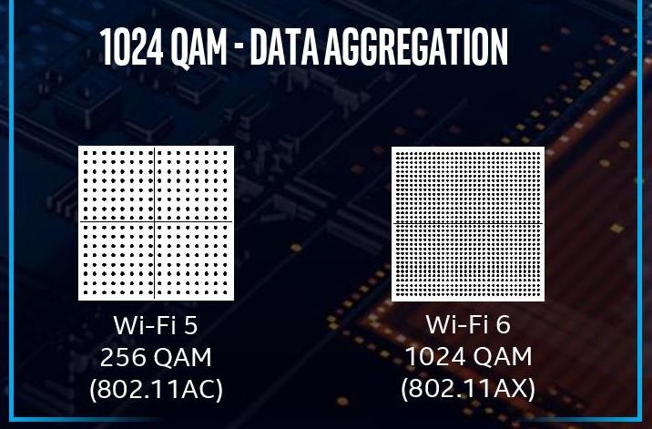
As an overarching technology, Wi-Fi 6 promises better bandwidth than standard Wi-Fi 5, as well as support for more devices on the same network. Technically this increased bandwidth comes down to data/time aggregation through the air as a benefit of OFDMA support, as well as 1024-QAM signaling design rather than 256-QAM signaling for increased throughput.

Wi-Fi 6 also has a lot of additional optional elements to the standard, which Intel believes will cause a good deal of confusion in the market. Naturally, Intel suggests that its partners that use a CNVi Wi-Fi 6 implementation also promote Wi-Fi 6 access points built on Intel’s platforms for simpler integration.
At this point in time, there are two main Wi-Fi 6 controllers: Intel’s AX200/AX201 2x2 CNVi module which uses the on-die enhancements, and Rivet Network’s AX1650 M.2 module which doesn’t use any of the on-die enhancements as it connects through a PCIe lane on the chipset. Technically both are built with the same silicon, as the companies are working together on the design, however Rivet is implementing its own acceleration techniques due to engines inside the hardware.
*The asterisk in the title of this page is because you still need external hardware in order to enable it, and to do it in the best way requires Intel-only hardware. You can use other vendor hardware, but you don’t need something special on the SoC to enable that.


107 Comments
View All Comments
repoman27 - Tuesday, July 30, 2019 - link
“Each CPU has 16 PCIe 3.0 lanes for external use, although there are actually 32 in the design but 16 of these are tied up with Thunderbolt support.”This isn’t quite right. The ICL-U/Y CPU dies do not expose any PCIe lanes externally. They connect to the ICL PCH-LP via OPI and the PCH-LP exposes up to 16 PCIe 3.0 lanes in up to 6 ports via HSIO lanes (which are shared with USB 3.1, SATA 6Gbps, and GbE functions). So basically no change over the 300 Series PCH.
The integrated Thunderbolt 3 host controller may well have a 16-lane PCIe back end on-die, and I’m sure the CPU floorplan can accommodate 16 more lanes for PEG on the H and S dies, but that’s not what’s going on here.
voicequal - Friday, August 2, 2019 - link
The SoC architecture shows a direct path for the Thunderbolt3 PCIe lanes to the CPU, with only USB2 going across OPI.. Whatever PCIe lanes are available on the PCH are in addition those available via TB3.https://images.anandtech.com/doci/14514/Blueprint%...
repoman27 - Tuesday, August 6, 2019 - link
The Thunderbolt 3 controller is part of the CPU die. There are four PCIe 3.0 x4 root ports connected to the CPU fabric that feed the Thunderbolt protocol converters connected to the Thunderbolt crossbar switch (the Converged I/O Router block in that diagram). The CPU exposes up to three (for Y-Series) or four (for U-Series) Thunderbolt 3 ports. The only way you can leverage the PCIe lanes on the back-end of the integrated Thunderbolt 3 controller is via Thunderbolt.The PCH is a separate die on the same package as the CPU die. The two are connected via an OPI x8 link operating at 4 GT/s which is essentially the equivalent of a PCIe 3.0 x4 link. The PCH contains a sizable PCIe switch internally which connects to the back-ends of all of the included controllers and also provides up to 16 PCIe 3.0 lanes in up to 6 ports for connecting external devices. These 16 lanes are fed into a big mux which Intel refers to as a Flexible I/O Adapter (FIA) along with all the other high-speed signals supported by the PCH including USB 3.1, SATA 6Gbps, and GbE to create 16 HSIO lanes which are what is exposed by the SoC. So there are up to 16 PCIe lanes available from the Ice Lake SoC package, all of which are provided by the PCH die, but they come with the huge asterisk that they are exposed as HSIO lanes shared with all of the other high-speed signaling capabilities of the PCH and provisioned by a PCIe switch that effectively only has a PCIe 3.0 x4 connection to the CPU.
This is not at all what Ian seemed to be describing, but it is the reality.
And the USB 2.0 signals for the Thunderbolt 3 ports do indeed come from the PCH, but they do not cross the OPI, they're simply routed from the SoC package directly to the Thunderbolt port. The Thunderbolt 3 host controller integrated into the CPU includes a USB 3.1 xHCI/xDCI but does not include a USB 2.0 EHCI.
poohbear - Tuesday, July 30, 2019 - link
I was looking at buying Dell's XPS 15.6" (7590 model), but with Project Athena laptops a few months away, i think i'll wait. Intel parts for solid reliability and unified drivers, and "4 hours of battery life with <30min of charging", those 2 on their own make the wait worth it for me!repoman27 - Tuesday, July 30, 2019 - link
“The connection to the chipset is through a DMI 3.0 x4 link...”Should be OPI x8 for U/Y Series.
“...Ice Lake will support up to six ports of USB 3.1 (which is now USB 3.2 Gen 1 at 5 Gbps)...”
They’re USB 3.1 Gen 2 ports, so it’s six USB 3.2 Gen 2 x 1 (10 Gbit/s) ports.
Roel9876 - Tuesday, July 30, 2019 - link
Well, for one, it is certainly not realistic to run single thread benchmarks on application that support multi threading. Realistically, most (all?) people will run the application multi threaded?HStewart - Tuesday, July 30, 2019 - link
As developer for many years, multiple threads are useful for handling utility threads and such - but IO is typically area which still has to single thread. Unless it has significantly change in API, it is very difficult to multi-thread the actual screen. And similar for disk io as resource.Arnulf - Tuesday, July 30, 2019 - link
"Our best guess is that these units assist Microsoft Cortana for low-powered wake-on voice inference algorithms ..."Our best guess is that these are designed for use by assorted three-letter agencies.
PeachNCream - Tuesday, July 30, 2019 - link
Open mics are totally okay. There is absolutely no privacy risk to you at all and you should never give it a second thought.ToTTenTranz - Tuesday, July 30, 2019 - link
With 4x TB3 connections available, I wonder if the maker of an external GPU box could develop a multiplexer that combined two TB3 connections into a PCIe 3.0 8x.This would significantly decrease some problems that eGPU owners are having due to relatively low CPU-GPU bandwidth.