Intel Unveils 10th Gen Core Ice Lake-U & Ice Lake-Y Mobile CPUs: 10nm Sunny Cove Later This Year
by Ian Cutress on May 29, 2019 8:00 AM EST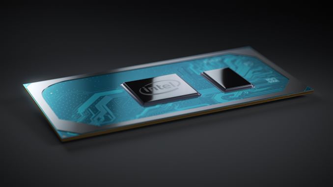
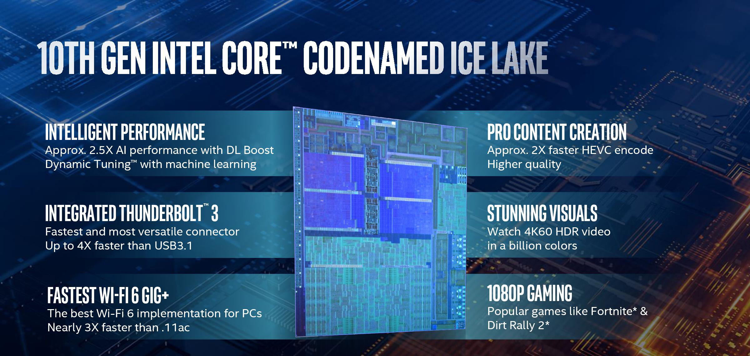
At Intel’s Keynote presentation here at Computex, the company finally lifted the lid on its first widely available new CPU design on its 10nm process, called Ice Lake. The official marketing name for these processors will be ‘Intel 10th Generation Core’, and will feature up to four CPU cores with Intel's new Sunny Cove architecture, new Gen11 graphics supplying up to 1TF of graphics/compute performance, and built in support for Wi-Fi 6 and Thunderbolt 3.
The story of Intel’s 10nm is a long and drawn out one, which we covered when we reviewed the first 10nm CPU, Cannon Lake, which only ended up in some limited Chinese system launch. Fast forward almost 2.5 years from when Intel officially announced it was shipping those 10nm CPUs and we have a full launch of Ice Lake, built on the company's greatly refined second-generation 10+ process. Intel spent a lot of its keynote presentation going through how it has driven the ecosystem and its ecosystem partners around developing systems with the new CPU in mind.
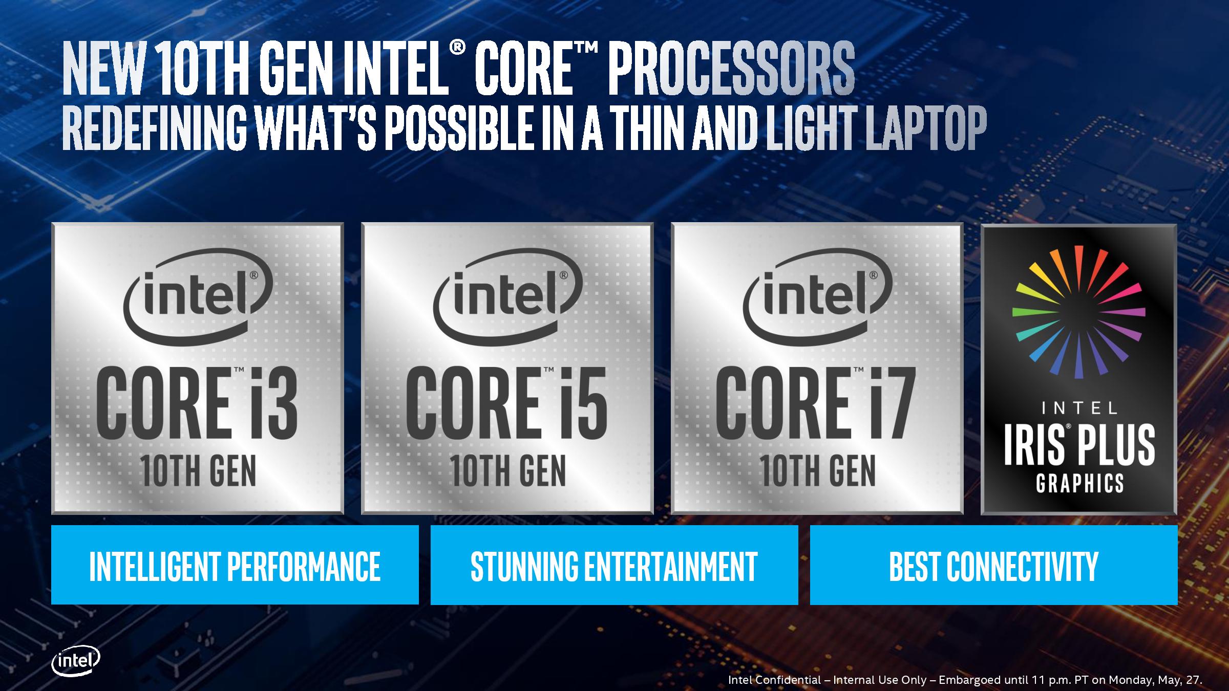
Intel is officially launching 11 different CPUs in the 10th Gen Core lineup, ranging from Core i3 to Core i7. Details on the specifications of those CPUs has not actually been released, which raises a number of questions of how much of a launch this actually is, however we do know that the best CPUs will have a turbo frequency up to 4.1 GHz and a top GPU frequency of 1.1 GHz. Users might consider this lower than 9th Gen mobile parts, which again raises questions. CPUs will be coming to market with 9W, 15W, and 28W variants.
Intel’s partners however have given us some specifications, and it shows in interesting adjustment in the naming scheme.
| OEM-Listed Intel Ice Lake 10nm CPUs | ||||||
| AnandTech | Core Threads |
Base Freq |
Turbo Freq |
IGP | TDP | Price (1ku) |
| i7-1065 G7 | 4C/8T | 1.3 GHz | 3.9 GHz | Yes | ? | ? |
| i5-1035 G1 | 4C/8T | ? | 3.7 GHz | Yes | ? | ? |
| i3-1005 G1 | 2C/4T | ? | 3.4 GHz | Yes | ? | ? |
At this point in time we’re not sure exactly what the ‘G7’ or ‘G1’ means in the name. It could be related to graphics, given that Intel will launch CPUs with 32 EUs, 48 EUs, or 64 EUs.
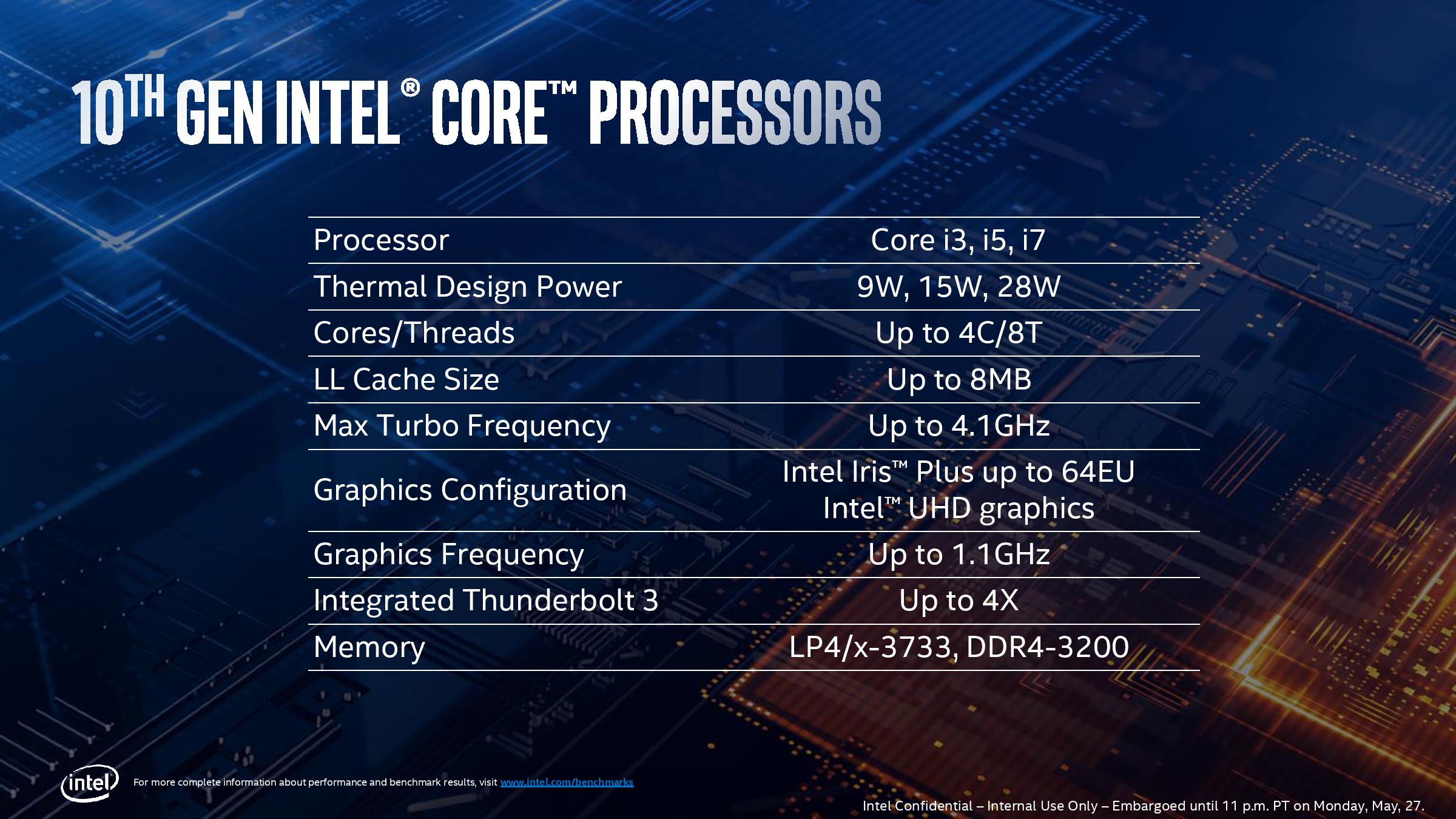
In accordance with their trio of TDPs, Intel has confirmed that there will be both Y-series and U-series Ice Lake parts. As a refresher, Intel's Y-series parts are their most compact, lowest-power chips, designed for passively cooled devices and other devices with limited cooling options, like 2-in-1s. Y-series chips have a nominal TDP of 9W – notably higher than the 5W TDPs for the current-generation Amber Lake-Y parts – and will be able to cTDP Up to 12W. Meanwhile Intel's U-series will, it appears, be the flag bearer for Ice Lake. These parts will have a nominal TDP of 15W, and can cTDP Up to 25W.
According to Intel's official product brief, both the U-series and Y-series parts will come with integrated GPUs with up to 64 EUs – this being particularly notable since the Y-series parts are going to be so low power. However it looks like Intel is going to split up the U-series a bit; 32 EU parts are listed as "Ice Lake U UHD", while 48 and 64 EU parts are "Ice Lake U Iris Plus". So Intel's Iris Plus branding will remain; and hopefully Iris Plus Ice Lake SKUs will be more common than today's Iris Plus parts.
Intel has discussed Ice Lake to a certain degree back in December and more recently at a private event, which we will be publishing after Computex to give it the attention it deserves. But the new core is designed to have more execution units, wider out-of-order windows, better load/store functionality, a bigger cache arrangement, and Intel states that this is good for an average 18% raw clock-for-clock performance uplift compared to the original Skylake core released in 2016.
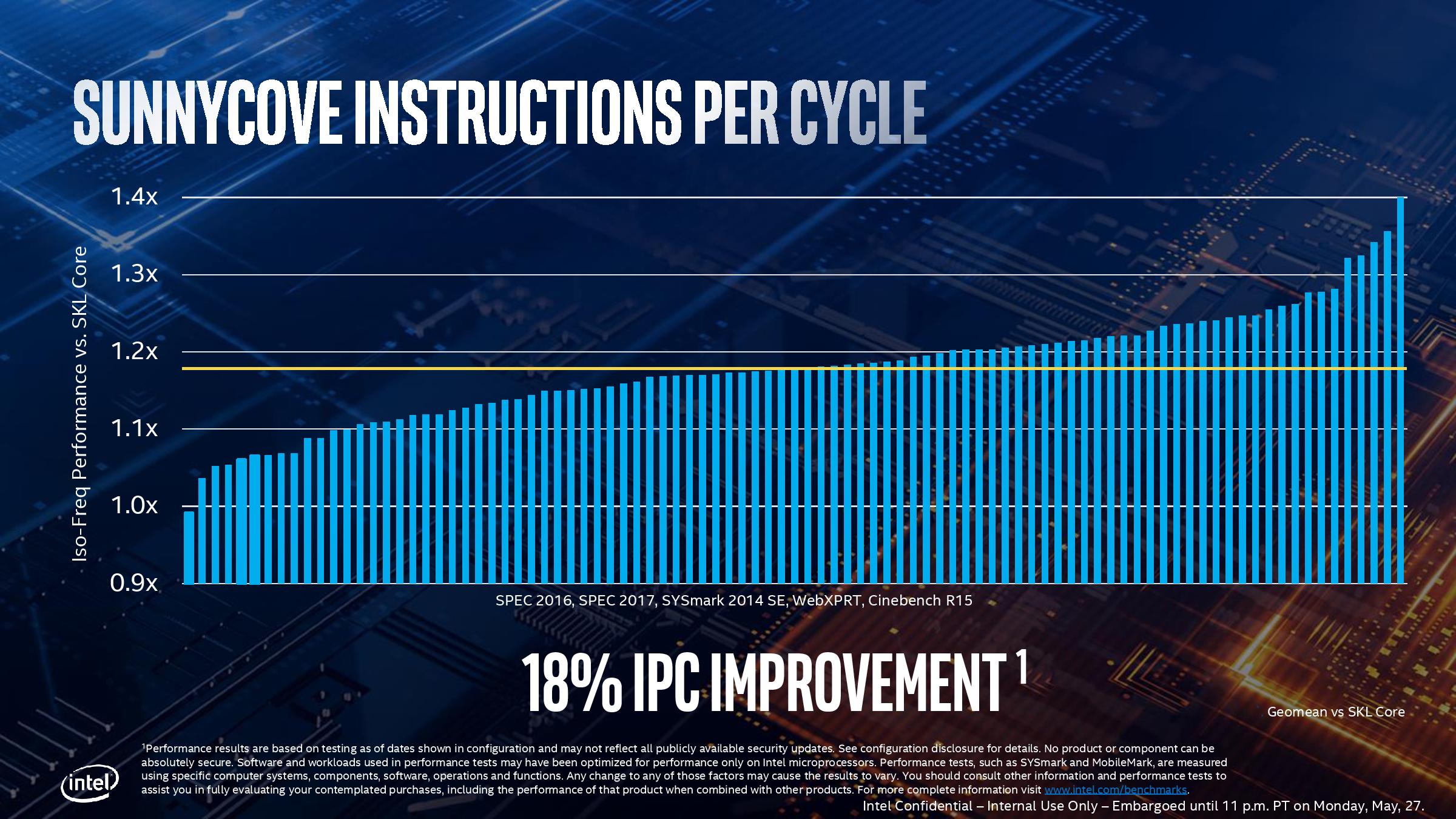
Users might be surprised about this 18% number, given that Intel has historically only provided low single digit boosts in recent generations. The reason for those single digit boosts comes down mainly to small parts of the core microarchitecture being widened. For Ice Lake, the doubling of the L2 cache, the increase in execution ports, and the dispatch capabilities of the front end of the core all provide big improvements. Intel also states that the pre-fetchers are improved, which also helps with that 18% IPC increase. It will be interesting to get hold of a system and to actually test/compare with Skylake, especially with all the security patches applied.
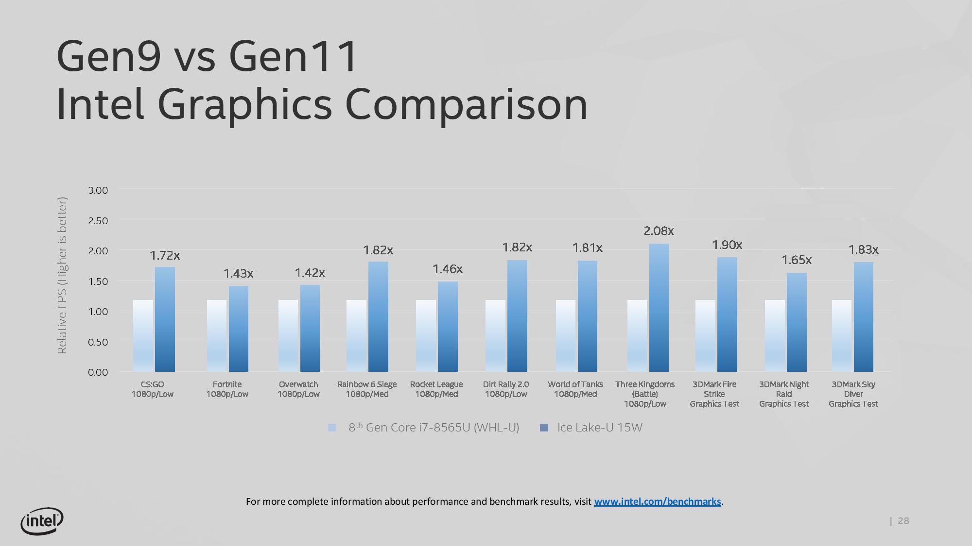
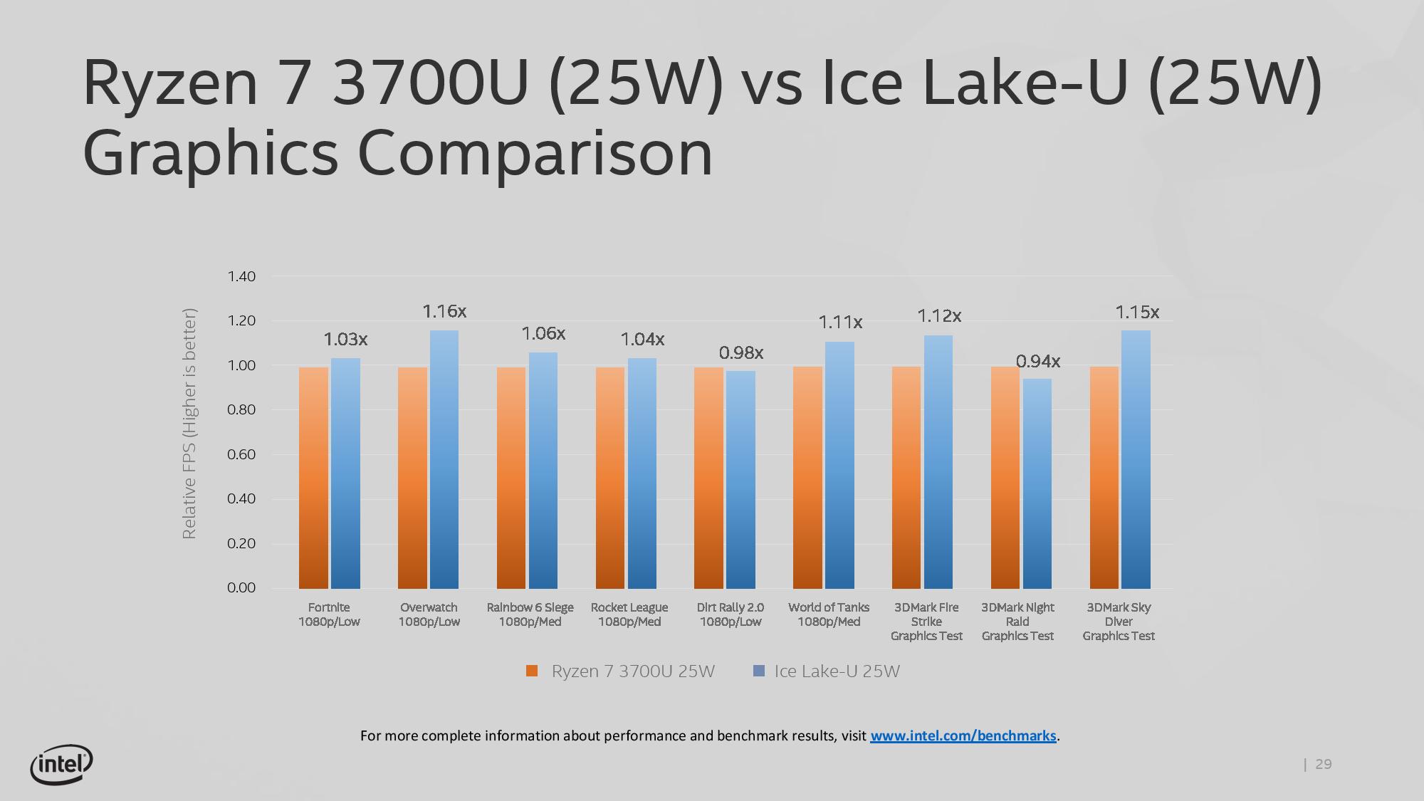
For graphics, Intel is stating that the best 10th Gen Core designs will be able to compete with what AMD has to offer with its mobile APU platforms. By increasing the number of execution units from 24 EUs to 64 EUs, Intel is promising over a 2x boost in graphics performance, which is facilitated by the better cache design on the CPU. The new graphics architecture, along with aggressive driver updates, should provide Intel better positioning in the thin-and-light gaming market. Benchmarks shown by Intel include many of the popular titles running today at 1920x1080 at either low or medium settings.
Core functionality aside, the new chips are also incorporating some of the latest I/O features. The biggest news here, of course, is integrated Thunderbolt 3 support for the on-chip 300 series mobile chip, finally doing away with the need for a separate PCIe-to-Thunderbolt controller. Not only will this save laptop OEMs space in their design, but as it's now a baseline feature of Intel's mobile chips, Thunderbolt 3 should become nearly ubiquitous across low-power laptops. Which considering that Thunderbolt 3 has been released to the world at large to be used as the basis for USB4, it's clear that Thunderbolt technology is quickly going to become a necessary feature for future laptops.
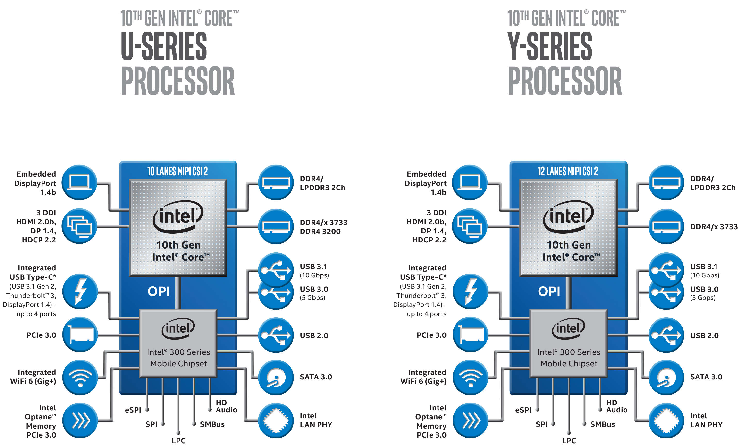
The other notable change here is support for Wi-Fi 6 (802.11ax), via Intel's increasingly well-established CNVi program. As with Intel's first-generation integrated Wi-Fi 5 functionality, Wi-Fi 6 is integrated in two parts. The Wi-Fi 6 Media Access Controller (MAC) is on Intel's chipset, meanwhile the RF hardware is on a separate companion module. Going this route is optimal for OEMs for regulatory reasons – the RF module can be certified separately – though it does mean they'll need to buy the RF module to make use of the processor's on-chip Wi-Fi capabilities. Interestingly, neither Intel nor the rest of the industry is wasting any time here; even though the Wi-Fi 6 standard hasn't been fully approved yet – it's still draft – it's already being integrated into hardware wide and far, including now mobile PC processors.
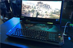
Overall, a number of ecosystem partners are at the Computex show with 10th Gen Core designs, including Dell, HP, Lenovo and others. For this new generation, Intel is also pushing its new Athena project, which we're covering in a separate article.
AnandTech's deep dive coverage of Intel 10th Gen Core will continue after Computex, with more details an analysis of the core microarchitecture. We're also working with Intel to get more access to Ice Lake platforms so we can provide a full testing profile of the new CPU family.
| Want to keep up to date with all of our Computex 2019 Coverage? | ||||||
 Laptops |
 Hardware |
 Chips |
||||
| Follow AnandTech's breaking news here! | ||||||


190 Comments
View All Comments
sorten - Wednesday, May 29, 2019 - link
Perhaps not exciting for everyone, but I'm hopeful because of the TB3 integration. I'm curious to see how this impacts the design of the Surface Pro 7. Unfortunately we're probably waiting until Spring 2020 to find out.jeremyshaw - Wednesday, May 29, 2019 - link
It's MSFT. I'd expect them to screw it up and just not enable TB3 or Type-C at all.sorten - Wednesday, May 29, 2019 - link
Unfortunately a real possibility. MS has become frustratingly conservative with hardware.katsetus - Wednesday, May 29, 2019 - link
Wait. Hold on.18% IPC increase but vs 15W i7-8665U the turbo frequency is down 900 MHz and base frequency is down 600 MHz (in case of the 1065 shown in the table). Going by turbo frequencies:
3.9/4.8=0.8125
0.8125*1.18=0.95875
So it is slower than i7-8665U. Only at the maximum 4.1 GHz, will speed parity be achieved. Although, yes, I am comparing it to the processor with the highest frequencies and hence price.
schujj07 - Wednesday, May 29, 2019 - link
Even the 8th Gen i5's have higher boost than 4.1GHz. Across the board the 10th Gen has lower clocks than the 8th Gen. Sure IPC increases will help mitigate the lower clock speed, but it is alarming how much lower the clocks are on 10nm+ from Intel. These low clocks are probably why there isn't a desktop CPU being released since it won't clock high enough to overtake the 9th Gen in absolute performance.flgt - Wednesday, May 29, 2019 - link
Saw an interesting lecture the other day. I didn't realize that all things being equal (ie you don't introduce a new structure like FinFET) that transistor performance no longer scales with nodes. You go to a smaller node you get a slower transistor, since the voltage can no longer scale at the same rate. So maybe something brilliant comes along but it looks like peak clock frequencies will be coming down. The only reason to scale at this point is economics, and even that is starting to become questionable if the large investment now required for the next node cannot show returns.abufrejoval - Wednesday, May 29, 2019 - link
Exactly, and it's been like that for many years already.Actually the 4.8 GHz Turbos on current Whiskey Lakes are just downright crazy and the result of Intel engineers spending years on getting that type of performance via physical tuning out of an "old engine". Those speeds also require 25 Watts on my i7-8565U, so they aren't sustained beyond a couple of seconds.
Most of that physical tuning simply cannot be carried over to a new process node: With EUV and everything else, it's just a completely new ball game.
Density gains hopefully will pay off the additional fab cost and allow widening those CPU structures for the IPC gains, additional cores and beefier GPUs.
Speed and density used to be linked in the good old days up to perhaps 45nm, but they have become rather antagonistic.
I won't predict speeds won't climb to 5GHz again (evidently you just need to leave the engineers alone with a new process node for long enough), but it's going to be harder with every shrink.
edzieba - Wednesday, May 29, 2019 - link
Not just performance, but cost/transistor has been increasing per node since 28nm. Expecting die shrinks to give you cheaper faster chips has not been true for many years now.name99 - Wednesday, May 29, 2019 - link
No it has not! If that were true, what do you think would be the cost of, say, an A12X chip with 12 billion transistors?Designing for each smaller node has become more expensive, but that’s a very different claim.
Meteor2 - Thursday, June 6, 2019 - link
It's a hell of a lot. Have you seen the price of an iPhone X or iPad Pro?!Both design and manufacture have become much more expensive. That's not a secret.