Arm's New Cortex-A77 CPU Micro-architecture: Evolving Performance
by Andrei Frumusanu on May 27, 2019 12:01 AM ESTThe Cortex-A77 µarch: Going For A 6-Wide* Front-End
The Cortex-A76 represented a clean-sheet design in terms of its microarchitecture, with Arm implementing from scratch the knowledge and lessons of years of CPU design. This allowed the company to design a new core that was forward-thinking in terms of its microarchitecture. The A76 was meant to serve as the baseline for the next two designs from the Austin family, today’s new Cortex-A77 as well next year’s “Hercules” design.
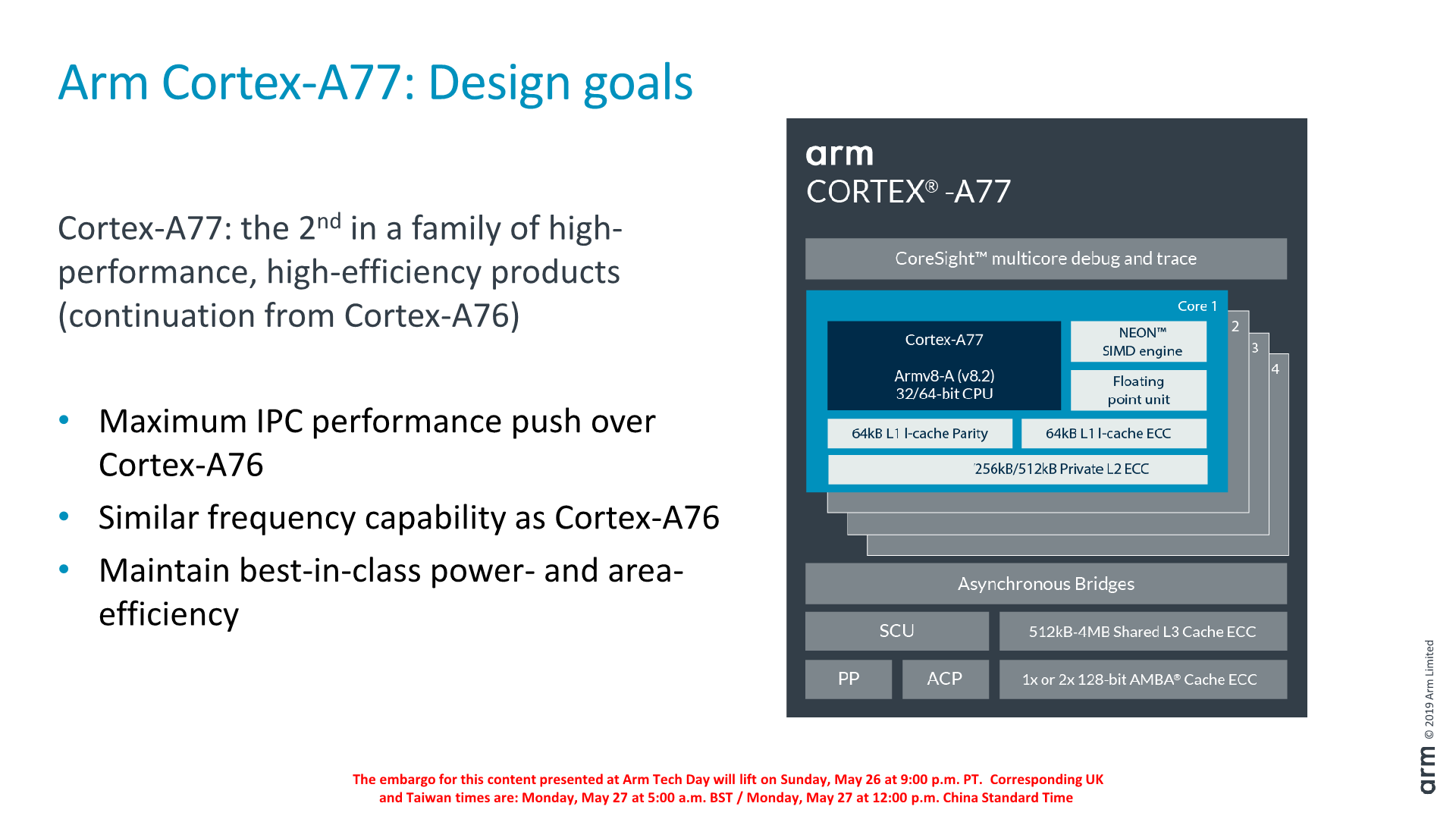
The A77 pushes new features with the primary goals of increasing the IPC of the microarchitecture. Arm’s goals this generation is a continuation of focusing on delivering the best PPA in the industry, meaning the designers were aiming to increase the performance of the core while maintaining the excellent energy efficiency and area size characteristics of the A76 core.
In terms of frequency capability, the new core remains in the same frequency range as the A76, with Arm targeting 3GHz peak frequencies in optimal implementations.

As an overview of the microarchitectural changes, Arm has touched almost every part of the core. Starting from the front-end we’re seeing a higher fetch bandwidth with a doubling of the branch predictor capability, a new macro-OP cache structure acting as an L0 instruction cache, a wider middle core with a 50% increase in decoder width, a new integer ALU pipeline and revamped load/store queues and issue capability.
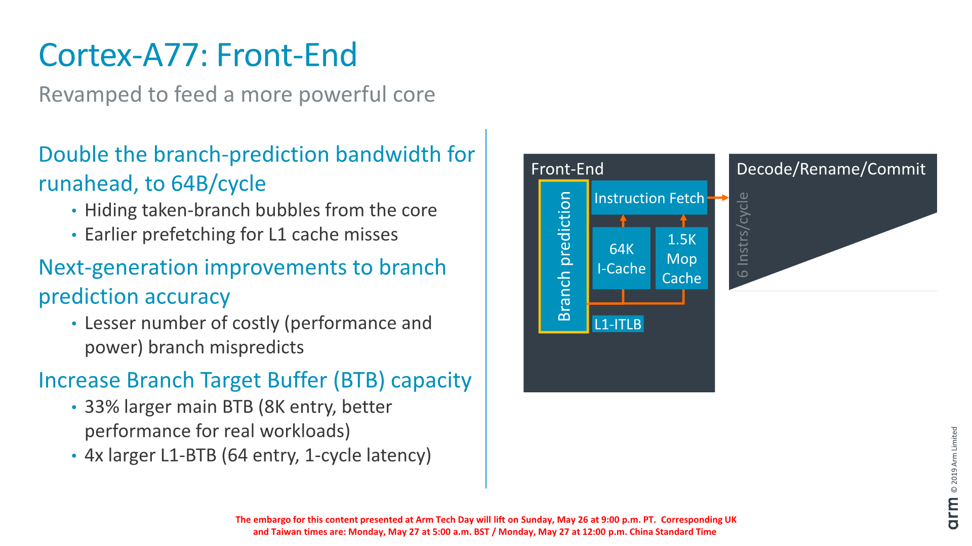
Dwelling deeper into the front-end, a major change in the branch predictor was that its runahead bandwidth has doubled from 32B/cycle to 64B/cycle. Reason for this increase was in general the wider and more capable front-end, and the branch predictor’s speed needed to be improved in order to keep up with feeding the middle-core sufficiently. Arm instructions are 32bits wide (16b for Thumb), so it means the branch predictor can fetch up to 16 instructions per cycle. This is a higher bandwidth (2.6x) than the decoder width in the middle core, and the reason for this imbalance is to allow the front-end to as quickly as possible catch up whenever there are branch bubbles in the core.
The branch predictor’s design has also changed, lowering branch mispredicts and increasing its accuracy. Although the A76 already had the a very large Branch Target Buffer capacity with 6K entries, Arm has increased this again by 33% to 8K entries with the new generation design. Seemingly Arm has dropped a BTB hierarchy: The A76 had a 16-entry nanoBTB and a 64-entry microBTB – on the A77 this looks to have been replaced by a 64-entry L1 BTB that is 1 cycle in latency.
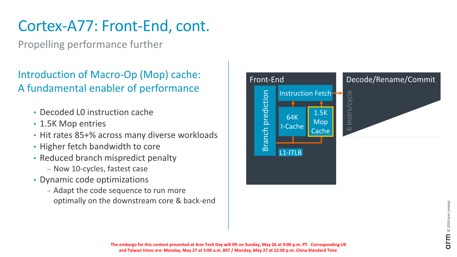
Another major feature of the new front-end is the introduction of a Macro-Op cache structure. For readers familiar with AMD and Intel’s x86 processor cores, this might sound familiar and akin to the µOP/MOP cache structures in those cores, and indeed one would be correct in assuming they have the similar functions.
In effect, the new Macro-OP cache serves as a L0 instruction cache, containing already decoded and fused instructions (macro-ops). In the A77’s case the structure is 1.5K entries big, which if one would assume macro-ops having a similar 32-bit density as Arm instructions, would equate to about 6KB.
The peculiarity of Arm’s implementation of the cache is that it’s deeply integrated with the middle-core. The cache is filled after the decode stage (in a decoupled manner) after instruction fusion and optimisations. In case of a cache-hit, then the front-end directly feeds from the macro-op cache into the rename stage of the middle-core, shaving off a cycle of the effective pipeline depth of the core. What this means is that the core’s branch mispredicts latency has been reduced from 11 cycles down to 10 cycles, even though it has the frequency capability of a 13 cycle design (+1 decode, +1 branch/fetch overlap, +1 dispatch/issue overlap). While we don’t have current direct new figures of newer cores, Arm’s figure here is outstandingly good as other cores have significantly worse mispredicts penalties (Samsung M3, Zen1, Skylake: ~16 cycles).
Arm’s rationale for going with a 1.5K entry cache size is that they were aiming for an 85% hit-rate across their test suite workloads. Having less capacity would take reduce the hit-rate more significantly, while going for a larger cache would have diminishing returns. Against a 64KB L1 cache the 1.5K MOP cache is about half the area in size.
What the MOP cache also allows is for a higher bandwidth to the middle-core. The structure is able to feed the rename stage with 64B/cycle – again significantly higher than the rename/dispatch capacity of the core, and again this imbalance with a more “fat” front-end bandwidth allows the core to hide to quickly hide branch bubbles and pipeline flushes.
Arm talked a bit about “dynamic code optimisations”: Here the core will rearrange operations to better suit the back-end execution pipelines. It’s to be noted that “dynamic” here doesn’t mean it’s actually programmable in what it does (Akin to Nvidia’s Denver code translations), the logic is fixed to the design of the core.
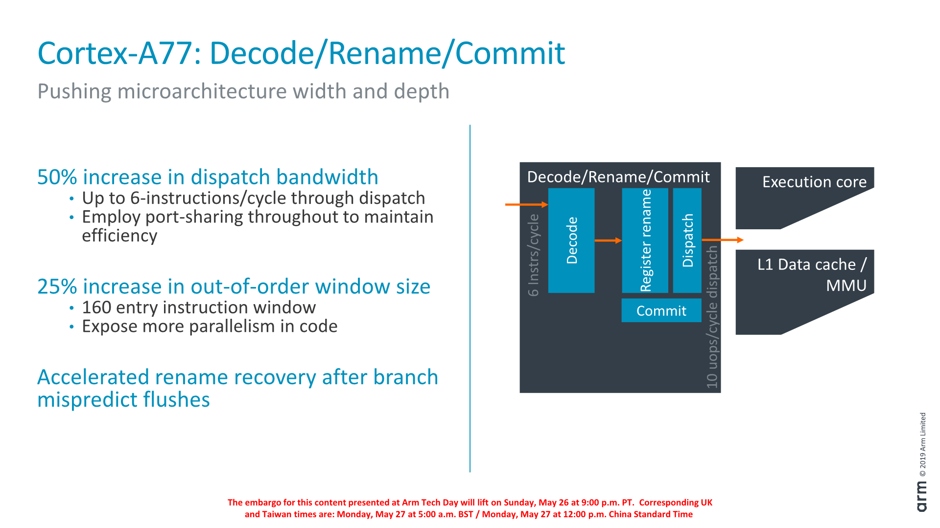
Finally getting to the middle-core, we see a big uplift in the bandwidth of the core. Arm has increased the decoder width from 4-wide to 6-wide.
Correction: The Cortex A77’s decoder remains at 4-wide. The increased middle-core width lies solely at the rename stage and afterwards; the core still fetches 6 instructions, however this bandwidth only happens in case of a MOP-cache hit which then bypasses the decode stage. In MOP-cache miss-cases, the limiting factor is still the decoder which remains at 4 instructions per cycle.
The increased width also warranted an increase of the reorder buffer of the core which has gone from 128 to 160 entries. It’s to be noted that such a change was already present in Qualcomm’s variant of the Cortex-A76 although we were never able to confirm the exact size employed. As Arm was still in charge of making the RTL changes, it wouldn’t surprise me if was the exact same 160 entry ROB.


108 Comments
View All Comments
Santoval - Monday, May 27, 2019 - link
Quite frankly, moving from a 4-wide to a 6-wide(!) design in the front end doesn't sound as an "evolutionary" design to me. That's an incredibly wide front end, wider even than when the A76 moved from 3-wide to 4-wide. I never expected ARM to go that wide, not so fast anyway. I wonder if the thermals will be affected, while the clocks should normally be lower.The addition of a macro-op L0 cache and the reworking of the backend are also quite significant.
frenchy_2001 - Monday, May 27, 2019 - link
I think Andrei referred to it as an evolution compared to the huge jump from A75 to A76.But you are right, each generation since A72 has been fairly different from the previous one.
The changes you pointed out also make more sense if you look at them for server/portable computers instead of phones.
Andrei Frumusanu - Tuesday, May 28, 2019 - link
Keep in mind that you can't just throw all those features in a core alone - the A76 was designed with A77 and Hercules in mind and in the pipeline.peevee - Tuesday, May 28, 2019 - link
"I wonder if the thermals will be affected, while the clocks should normally be lower."L0 MOP-cache eliminates 85% of the work here, so the new wide decoders will mostly sit idle, but quickly filling in the queue when a branch jumps out of L0 window.
Main Sandy Bridge enhancement, finally. And makes total sense given that A8.2 became just about as huge as Sandy Bridge with its AVX1, necessitating huge power-hungry decoders. RISC my a$$...
Wardrive86 - Monday, May 27, 2019 - link
Has Arm ever stated why they went back to an Architectural register file after using a physical register file for the A73 and A75? Its interesting that they get the performance they do with such a small one... relatively speakingWardrive86 - Monday, May 27, 2019 - link
Not to double post but I wonder if it is just differing design philosophies between the Austin and Sophia teams.Andrei Frumusanu - Tuesday, May 28, 2019 - link
Yes, it's an implementation/electrical engineering question between both teams.blu42 - Tuesday, May 28, 2019 - link
Perhaps it could be more due to different design philosophies between Austin and Sophia design centres?jcc5169 - Monday, May 27, 2019 - link
It's so funny to me that Anandtech now goes out of its way to talk about everyone but AMDRyan Smith - Tuesday, May 28, 2019 - link
Beg your pardon?https://www.anandtech.com/show/14407/amd-ryzen-300...
https://www.anandtech.com/show/14412/amd-teases-fi...
And that's just in the last 36 hours.