Arm's New Cortex-A77 CPU Micro-architecture: Evolving Performance
by Andrei Frumusanu on May 27, 2019 12:01 AM EST
2018 was an exciting year for Arm’s own CPU designs. Last year in May we saw the release of the Cortex-A76 and the subsequent resulting silicon in the form of the Kirin 980 as well as Snapdragon 855 SoCs. We were very impressed by the IP, and Arm managed to deliver on all its performance, efficiency and area promises, resulting in some excellent SoCs and devices powering most of 2019’s flagship devices.
This year we follow-up with another TechDay disclosure, and this time around we’re uncovering Arm’s follow-up to the Cortex-A76: the new Cortex-A77. The new generation is a direct evolution of last year’s major microarchitecture introduction, and represents the second instance of Arm’s brand-new Austin core family. Today we’ll analyse how Arm has pushed the IPC of its new microarchitecture and how this will translate into real performance for upcoming late-2019/early-2020 SoCs and devices.
Deimos turns to Cortex-A77
The announcement of the Cortex-A77 doesn’t come as a surprise as Arm continues on their traditional annual IP release cadence. In fact today is not the first time that Arm has talked about the A77: In August of last year Arm had teased the CPU core when releasing its performance roadmap through 2020:

Codenamed as “Deimos”, the new Cortex-A77 picks up where the Cortex-A76 left off and follows Arm’s projected trajectory of delivering a continued solid 20-25% CAGR of performance uplift with each generation of Arm’s new Austin family of CPUs.
Before we dwell into the new Cortex-A77, we should take a look back at how the performance of the A76 has evolved for Arm:
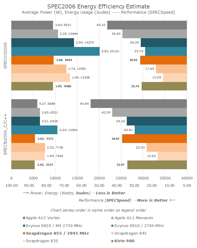
The A76 has certainly been a hugely successful core for Arm and its licensees. The combination of the brand-new microarchitecture alongside the major improvements that the 7nm TSMC process node has brought some of the biggest performance and efficiency jumps we’ve ever seen in the industry.
The results is that the Kirin 980 as well as the Snapdragon 855 both represented major jumps over their predecessors. Qualcomm has proclaimed a 45% leap in CPU performance compared to the previous generation Snapdragon 845 with Cortex-A75 cores, the biggest generational leap ever.
While the performance increase was notable, the energy efficiency gains we saw this generation was even more impressive and directly resulted in improved battery life of devices powered by the new Kirin and Snapdragon SoCS.
While the A76 performed well, we should remember that it does have competition. While Samsung’s own microarchitecture this year with the M4 has lessened the performance/efficiency gap, the Exynos CPU still largely lags behind by a generation, even though this difference is amplified by a process node difference this year (8nm vs 7nm). The real competition for Arm here lies with Apple’s CPU design teams: Currently the A11 and A12 still hold a large performance and efficiency lead that amounts to roughly two microarchitecture generations.
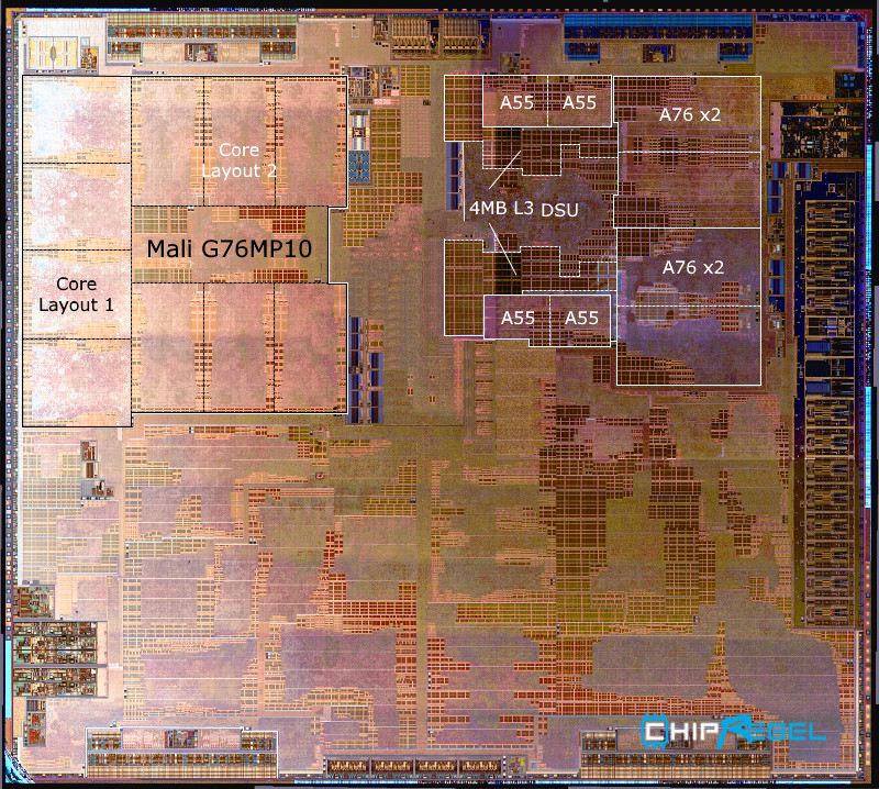
Die shot credit: ChipRebel - Block labelling: AnandTech
One of Arm’s fortes however remains in delivering the best PPA in the industry. Even though the A76’s performance didn’t quite match Apple’s, it managed to achieve outstanding efficiency with incredibly small die area sizes. In fact, this is a conscious design decision by Arm as power efficiency and area efficiency are among the top priorities for Arm’s licensees.
The Cortex-A77: A Top-Level Overview
The Cortex-A77 being a direct microarchitectural successor to the A76 means the new core largely stays in line with the predecessor’s features. Arm states that the core was built in mind with vendors being able to simply upgrade the SoC IP without much effort.

In practice what this means is that the A77 is architecturally aligned with its predecessor, still being an ARMv8.2 CPU core that is meant to be paired with a Cortex-A55 little CPU inside of a DynamIQ Shared Unit (DSU) cluster.
Fundamental configuration features such as the cache sizes of the A77 also haven’t changed compared to its predecessor: We’re still seeing 64KB L1 instruction and data caches, along with a 256 or 512KB L2 cache. It’s interesting here that Arm did design the option for an 1MB L2 cache for the infrastructure Neoverse N1 CPU core (Which itself is derived from the A76 µarch), but chooses to stay with the smaller configuration options on the client (mobile) CPU IP.
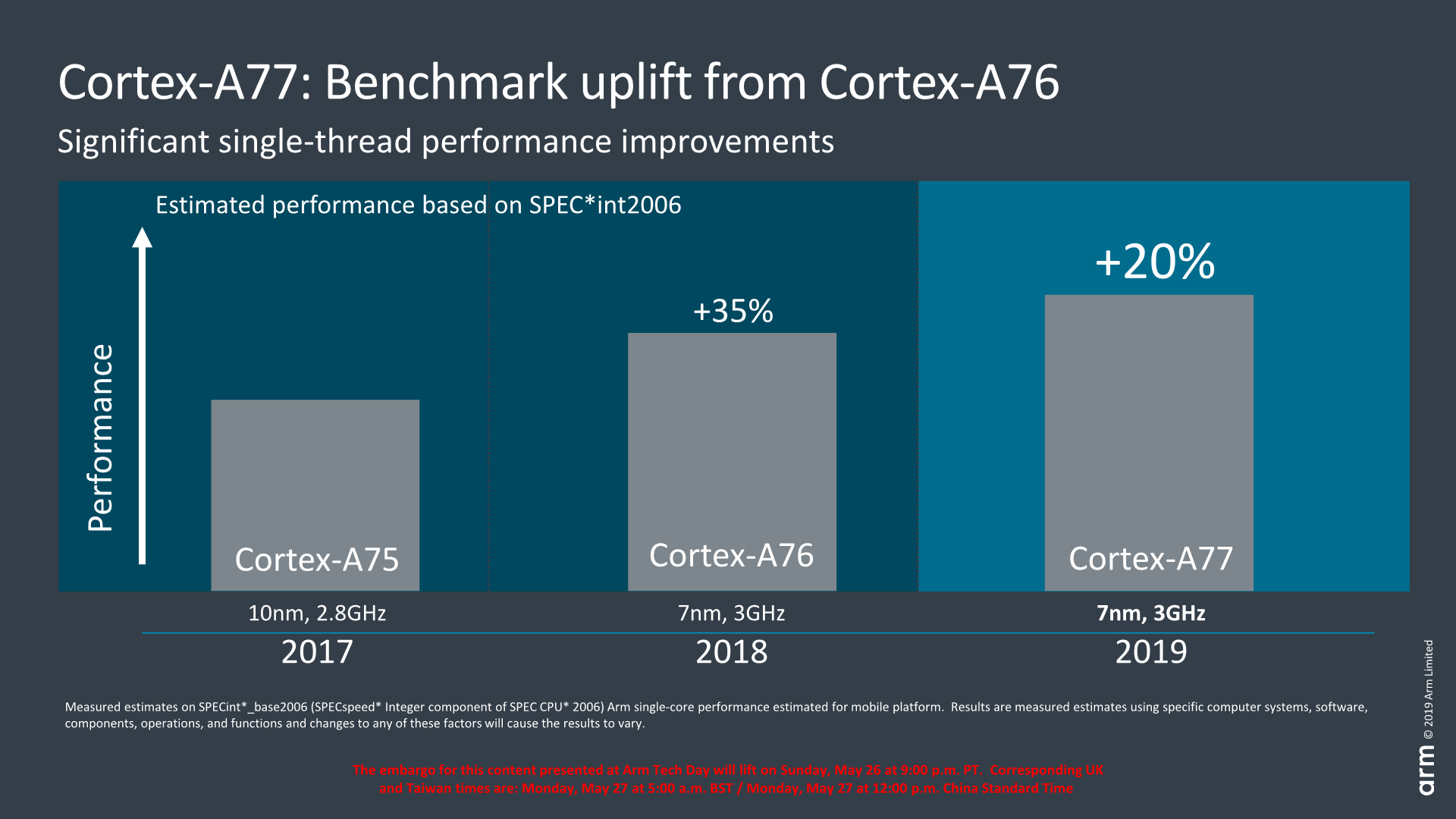
As an evolution of the A76, the A77 performance jump as expected won’t be quite as impressive, both from a microarchitecture perspective, but also from an absolute performance standpoint as we’re not expecting large process node improvements for the coming SoC generation.
Here the A77 is projected to still be productised on 7nm process nodes for most customers, and Arm is proclaiming a similar 3GHz peak target frequency as its predecessor. Naturally since frequency isn’t projected to change much, this means that the core’s targeted +20% performance boost can be solely attributed to the IP’s microarchitectural changes.
To achieve the IPC (Instructions per clock) gains, Arm has reworked the microarchitecture and introduced clever new features, generally beefing up the CPU IP to what results in a wider and more performant design.


108 Comments
View All Comments
Santoval - Monday, May 27, 2019 - link
Quite frankly, moving from a 4-wide to a 6-wide(!) design in the front end doesn't sound as an "evolutionary" design to me. That's an incredibly wide front end, wider even than when the A76 moved from 3-wide to 4-wide. I never expected ARM to go that wide, not so fast anyway. I wonder if the thermals will be affected, while the clocks should normally be lower.The addition of a macro-op L0 cache and the reworking of the backend are also quite significant.
frenchy_2001 - Monday, May 27, 2019 - link
I think Andrei referred to it as an evolution compared to the huge jump from A75 to A76.But you are right, each generation since A72 has been fairly different from the previous one.
The changes you pointed out also make more sense if you look at them for server/portable computers instead of phones.
Andrei Frumusanu - Tuesday, May 28, 2019 - link
Keep in mind that you can't just throw all those features in a core alone - the A76 was designed with A77 and Hercules in mind and in the pipeline.peevee - Tuesday, May 28, 2019 - link
"I wonder if the thermals will be affected, while the clocks should normally be lower."L0 MOP-cache eliminates 85% of the work here, so the new wide decoders will mostly sit idle, but quickly filling in the queue when a branch jumps out of L0 window.
Main Sandy Bridge enhancement, finally. And makes total sense given that A8.2 became just about as huge as Sandy Bridge with its AVX1, necessitating huge power-hungry decoders. RISC my a$$...
Wardrive86 - Monday, May 27, 2019 - link
Has Arm ever stated why they went back to an Architectural register file after using a physical register file for the A73 and A75? Its interesting that they get the performance they do with such a small one... relatively speakingWardrive86 - Monday, May 27, 2019 - link
Not to double post but I wonder if it is just differing design philosophies between the Austin and Sophia teams.Andrei Frumusanu - Tuesday, May 28, 2019 - link
Yes, it's an implementation/electrical engineering question between both teams.blu42 - Tuesday, May 28, 2019 - link
Perhaps it could be more due to different design philosophies between Austin and Sophia design centres?jcc5169 - Monday, May 27, 2019 - link
It's so funny to me that Anandtech now goes out of its way to talk about everyone but AMDRyan Smith - Tuesday, May 28, 2019 - link
Beg your pardon?https://www.anandtech.com/show/14407/amd-ryzen-300...
https://www.anandtech.com/show/14412/amd-teases-fi...
And that's just in the last 36 hours.