TSMC: Most 7nm Clients Will Transition to 6nm
by Anton Shilov on May 1, 2019 6:30 PM EST- Posted in
- Semiconductors
- TSMC
- 7nm
- 6nm
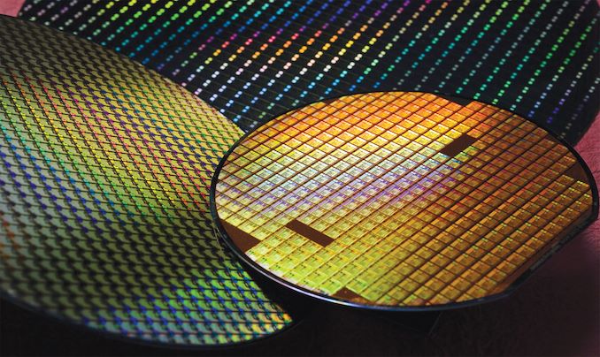
In this week's quarterly earnings conference call, TSMC’s revealed that the company expects most of its 7nm "N7" process customers to eventually transition to its forthcoming 6nm "N6" manufacturing node. The upcoming node will use the same design rules as the N7 node, making it easier for customers to transition to the newer, denser node. And, if TSMC's predictions come true, N6 is now on the path towards becoming another widely-utilized, long-serving process node for the company.
In comments made during the quarterly call, CC Wei, TSMC's CEO and vice chairman noted that “most of the customers in the N7 will move to N6.” In fact it sounds like TSMC's N6 node is set to become another one of TSMC's popular, high volume nodes, with Wei further stating that “from that day on probably, the N6 will pick up all the momentum and pick up all the volume production.”
As previously reported, TSMC’s N6 process technologies adopts extreme ultraviolet lithography (EUVL) to lower manufacturing complexity by reducing the number of exposures required for multi-patterning (which is needed today as TSMC’s N7 uses solely DUV lithography). While TSMC's N7+ uses up to four EUVL layers, its N6 expands it up to five layers, whereas N5 expands usage of EUVL all the way to 14 layers.
UPDATE: Correcting the number of EUV layers used by N6 and N7.
While TSMC’s N6 uses new production equipment and offers 18% higher transistor density than the company’s N7 manufacturing technology, N6 uses the same design rules as N7 and enables designers of chips to re-use the same design ecosystem (e.g., tools, etc.), which will allow them to lower development costs. By contrast, N7+ uses different design rules, but also provides more advantages than N6 when compared to N7.
| Advertised PPA Improvements of New Process Technologies Data announced by companies during conference calls, press briefings and in press releases |
|||||||||
| TSMC | |||||||||
| 16FF+ vs 20SOC |
10FF vs 16FF+ |
7FF vs 16FF+ |
7FF vs 10FF |
7FF+ vs 7FF |
6FF vs 7FF |
5FF vs 7FF |
|||
| Power | 60% | 40% | 60% | <40% | 10% | ? | 20% | ||
| Performance | 40% | 20% | 30% | ? | same (?) | ? | 15% | ||
| Area Reduction | none | >50% | 70% | >37% | ~17% | ~15% | 45% | ||
While TSMC’s partners have adopted both N7 and N7+ processes and the world’s largest contract maker of chips expects the two technologies to contribute over 25% of its wafer revenue in 2019, the former looks to be somewhat more popular that the latter. Meanwhile, TSMC projects that most of its customers who use N7 today will migrate to N6 and then to N5 skipping the N7+. Considering how widespread N7 is going to get, N6 will likely be quite popular as well.
Related Reading:
- TSMC Reveals 6 nm Process Technology: 7 nm with Higher Transistor Density
- TSMC’s 5nm EUV Making Progress: PDK, DRM, EDA Tools, 3rd Party IP Ready
- TSMC: 7nm Now Biggest Share of Revenue
- TSMC: First 7nm EUV Chips Taped Out, 5nm Risk Production in Q2 2019
- TSMC Details 5 nm Process Tech: Aggressive Scaling, But Thin Power and Performance Gains


39 Comments
View All Comments
jordanclock - Wednesday, May 1, 2019 - link
Essentially zero. It takes way too much time to rework an architecture for a smaller process node than AMD would have had, even if they were the very first to be informed of this new node.coburn_c - Wednesday, May 1, 2019 - link
u wot m8ZolaIII - Thursday, May 2, 2019 - link
Using same design rules actually means you don't have to touch previously lay down design, you just re root it because N6 is the same N7 with used different denser lib.levizx - Friday, May 3, 2019 - link
It is NOT a smaller nod. And since design rules are the same, it's very possible Zen2+, likely used on APUs in late 2020 or later, are using a variant of this.AMD is not using vanilla N7FF in the first place.
Colorado_Chips - Wednesday, May 1, 2019 - link
If Zen2 is N7 (and not, say, N7+), then Zen2+ is certain to be N6. No redesign, just pay for masks and do the post-silicon characterization. Meanwhile, the design team is working on Zen3 in N5. It's a no-brainer. Looks a lot like Zen to Zen+ from 14nm to 12nm.Colorado_Chips - Wednesday, May 1, 2019 - link
Okay, just saw a slide showing Zen3 in 7nm+, soooo ... never mind.Eris_Floralia - Wednesday, May 1, 2019 - link
No. Zen2 isn't on N7+. And N6 is 2020Q1 risk production. There's nothing called Zen2+.levizx - Wednesday, May 8, 2019 - link
Then what do you think Ryzen 4000 APU, which certainly wouldn't be out before late 2020, would be called?ET - Thursday, May 2, 2019 - link
Zen 2+ has never been mentioned. Zen 3 will come after Zen 2.That said, I can see where AMD might want to use this, for example for GPUs or APUs after Renoir. For a mainstream APU it seems reasonable to use a mainstream process that nevertheless is denser than 7nm. A long term entry level 4C/8T APU could be a nice N6 option.
lightningz71 - Thursday, May 2, 2019 - link
If TSMC is telling the truth that N6 is essentially a drop in "fit" for an N7 design, then, AMD MIGHT, and I do mean MIGHT bother to switch the 4000 series APUs to N6 to increase wafer yield. It is suspected that the next batch of APUs from AMD will aim for higher performance than the current ones, and will require more cores and more cache, on top of having a substantial iGPU section. That's going to be a largish design that will absolutely benefit from having maximum circuit density to be able to also fit into the existing package sizes they are using in the mobile space to keep integrator costs low.If it really is that much denser, that would allow AMD to make an APU that has 8 cores, 16MB of L3, and a 12 or so CU implementation of NAVI or VEGA+ and still come in smaller than the 2700u that's currently on the market.