The Samsung Galaxy S10+ Snapdragon & Exynos Review: Almost Perfect, Yet So Flawed
by Andrei Frumusanu on March 29, 2019 9:00 AM ESTThe Exynos 9820 SoC - A New Tri-CPU Design
While we know quite a lot about the new Snapdragon 855, information on the new Exynos 9820 has been extremely scarce given S.LSI’s more closed nature. What we know is that the new chip brings with it a new tri-CPU group design and a few vague mentions about its performance and efficiency claims. The chip was announced back in November and I wasn’t too hopeful based on the quoted marketing numbers – the figures needed to be better in order to be able to compete with the Kirin 980 and Snapdragon 855, at least on paper.
Probably the biggest wildcard for the Exynos 9820 is its 8nm LPP manufacturing node. Qualcomm this year had opted to switch over to TSMC’s 7nm manufacturing node for the Snapdragon 855, and the decision looks to be linked to the indisputable superiority of the node.
| Samsung Exynos SoCs Specifications | ||
| SoC |
Exynos 9820 |
Exynos 9810 |
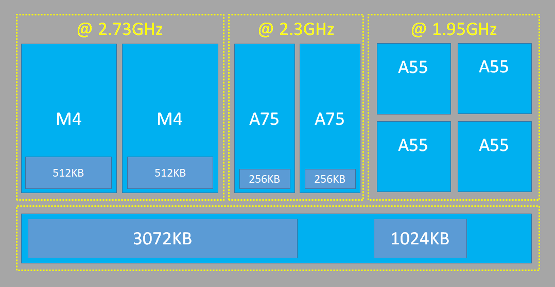
| CPU | 2x M4 @ 2.73 GHz 2x 512KB pL2 2x Cortex A75 @ 2.31 GHz 2x 256KB pL2 4x Cortex A55 @ 1.95 GHz No pL2's Shared complex sL3 @ 4MB |
4x M3 @ 1c2.7 / 2c2.3 / 4c1.8 GHz 4x 512KB pL2 4096KB sL3 4x Cortex A55 @ 1.8 GHz no pL2 512KB sL3 |
| GPU | Mali G76MP12 @ 702MHz | Mali G72MP18 @ 572MHz |
| Memory Controller |
4x 16-bit CH LPDDR4X @ 2093MHz |
4x 16-bit CH LPDDR4X @ 1794MHz |
| ISP | Rear: 22MP Front: 22MP Dual: 16MP+16MP |
Rear: 24MP Front: 24MP Dual: 16MP+16MP |
| Media | 8K30 & 4K150 encode & decode H.265/HEVC, H.264, VP9 |
10bit 4K120 encode & decode H.265/HEVC, H.264, VP9 |
| Integrated Modem | Shannon 5000 Integrated LTE (Category 20/13) DL = 2000 Mbps 8x20MHz CA, 256-QAM UL = 316 Mbps 3x20MHz CA, 256-QAM |
Shannon 359 Integrated LTE (Category 18/13) DL = 1200 Mbps 6x20MHz CA, 256-QAM UL = 200 Mbps 2x20MHz CA, 256-QAM |
| Mfc. Process | Samsung 8nm LPP |
Samsung 10nm LPP |
ChipRebel a few weeks ago was able to tear down a Galaxy S10 with the Exynos 9820 and take some great die shot pictures revealing the innards of the new chip.
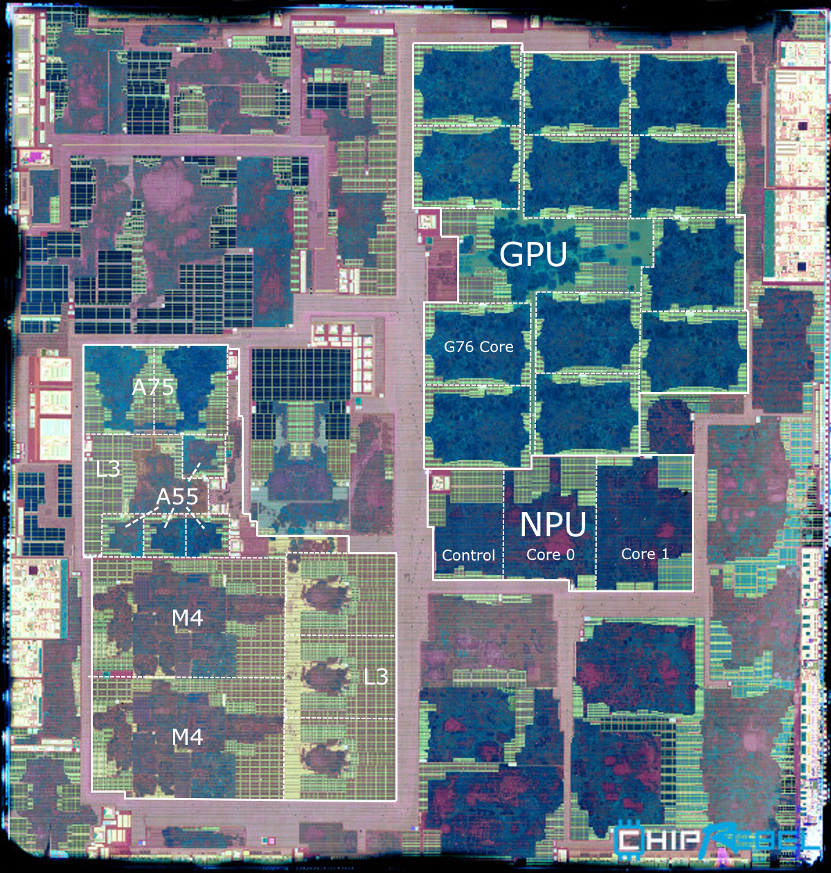
Die shot: Chip Rebel - Annotations/labelling: Andrei @ AnandTech
The one thing that immediately jumps out is the fact that at 127mm², Samsung new chip is extremely large compared to the 73mm² Snapdragon 855. At least in terms of die size, I don’t remember the differences between two SoCs of a generation to have ever been this large.
The new SoC sees the usage of Samsung’s fourth generation CPU core, the M4. The new CPU is codenamed Cheetah, a quite obvious nod to the design team which consists of former AMD folks who were responsible for the big cat line-up of CPU cores.
The CPU cluster is completely re-arranged when compared to last year’s Exynos 9810. A notorious issue with the prior chip was that the little CPU cores weren’t under the same cache hierarchy as the M3 cores, owning to a similar design as found in past SoCs where cache coherency between CPUs was done through the interconnect between them. The new Exynos 9820 now has a similar unified cache hierarchy as found in Arm’s DynamIQ designs, although there are some important differences.
Instead of four big cores, the Exynos 9820 employs only two – the two Cheetah M4 cores clock up to 2.73GHz and are accompanied by two Cortex A75 cores at 2.3GHz and four Cortex A55 cores at 1.95GHz. In fact, the Exynos 9820 is the first tri-CPU cluster/group SoC which actually consists of three different CPU microarchitectures. In practice, the Exynos 9820 is more similar to the Kirin 980 in this regard, just instead of the middles cores being power optimised variants of the big core, it’s just outright a smaller microarchitecture.
Samsung configures the M4 cores with 512KB private L2 caches while the A75’s get 256KB L2’s. Interestingly, Samsung again opted to not configure the A55 cores with L2 caches, instead opting to rely on their custom 1MB L3 slice. It’s here that things become interesting and a bit more exotic than Arm’s DSU. Samsung new L3 cache consists of two different structures. The M4 cores seemingly have access to 3x1MB slices which look to be very similar to the design of the L3 slices found on the Exynos 9810. However on top of this Samsung has a dedicated 1MB slice to which the Cortex A75 and A55 cores have access to. The M4 cores also have access to this 1MB slice, whereas the Cortex don’t have access to the other 3MB of L3.
As of yet I didn't manage to determine how the L3 slices are clocked. On the Exynos 9810 the L3 was on the same clock plane as the big cores, and this might also be the case for the 3MB of the Exynos 9820 as well, but I’m fairly certain the 1MB slice will have a different design and clock plane.
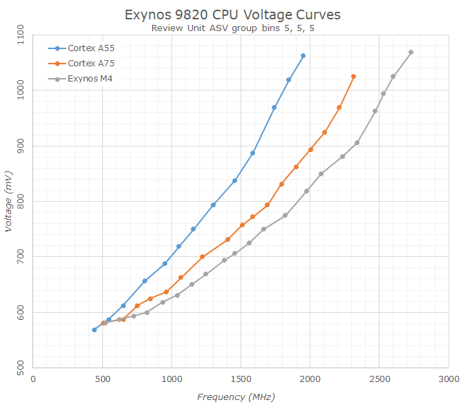
I extracted the voltage tables for my Galaxy S10+ unit which ended up with a mid-tier bin of 5 (Out of usually 13 groups) which is just slightly below what should be the median distribution. Samsung is still extremely aggressive in terms of the peak voltages, going over 1V for all three CPU clusters. The M4 cores went up to 1062mV at 2.73GHz on my unit, and there’s an evident kink in the voltage curve after 2.34GHz where the CPU requires a steep increase in voltage. I didn’t manage to read out the exact voltages on my Snapdragon 855 unit, but it did have a peak voltage on the prime cores at 2.84GHz of 1V, meaning already just by voltage alone the Snapdragon should have an efficiency advantage.
We see similar steep curves on the A75 and in particular the A55 cores. Last year for the Exynos 9820 I argued that it was better to remain on the A55 cores at very high frequencies and high voltages than to power on the M3 cores, but for the Exynos 9820 I have to wonder why Samsung opted to clock the A55 as high, as there’s again a very big efficiency deficit in the top frequencies. If and how this all works out, is going to depend on the scheduler and how it handles transitions between the CPUs.

Looking at Samsung’s scheduler power tables, we see some odd characteristics. According to this, the A75 cores actually aren’t more efficient than the M4 cores, except for at the lower frequencies. What is really irking me however is I can’t seem to understand why the A55 cores are marked to be as high In performance, reaching 42% of the maximum load scale. This characteristic can also be found on the Snapdragon 855. The source code marks that the performance scale is determined by MIPS, which I think is an extremely weird metric to normalise performance with. The reason could be related to how PELT works on the Exynos 9820, however I’ll get back to this topic on the system performance page later in the piece.
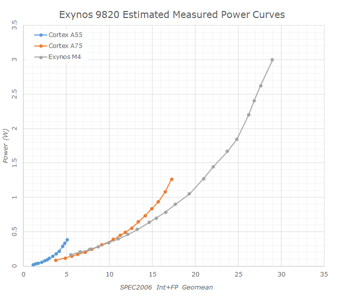
A more real-world power-performance curve would look as above. Here I actually went ahead and measured the SPEC performance and power at their respective peak points and normalised the curves based on this. The Cortex A55 cores in particular see a big down-shift in their relative performance.

Looking at the same data when normalising the x-axis for perf/W instead of absolute power, we again see in more obvious manner that the M4 cores should very much be quite a lot more efficient than the A75 cores at the same performance, at least for the vast majority of the A75’s upper frequency range. Similarly, the A75’s should be a ton more efficient the A55 cores at the upper performance points of the A55’s. The power figures here consider the active power (load minus idle) of the whole platform, not merely just the CPU cores. This would be a case where race-to-idle at higher power points is actually more efficient than staying on the efficient CPU cores, because of overhead of the rest of the SoC and platform such as memory controllers, DRAM, and PMIC.
It’ll be interesting so see how the Exynos 9820 fares in efficiency, as it has seemingly a large dynamic range in efficiency points.
The GPU on the new SoC is Arm’s new Mali G76 in a 12-core configuration. We had already seen the same GPU in a MP10 configuration employed in HiSilicon’s Kirin 980. In the Exynos implementation, Samsung is clocking the GPU up to at up to 702MHz which is quite higher than the 572MHz of last year’s G72MP18. I’ve noted that the voltages are quite low – 668mV at peak frequency and the voltage curve is quite shallow, meaning efficiency at lower frequencies/performance points won’t be all that much better.
A big new addition this year for Samsung is a new dedicated NPU. The new in-house IP by Samsung is quite intriguing. The company had presented the block as ISSCC this year, revealing some of its high-level workings. The block consists of 3 units: a central control block with a CPU, and two cores which contain the MAC engines. Samsung describes the block as configured in a “butterfly” structure, which specifically addresses in the way the dual-core configuration is set up. In terms of capability, there’s 1024 MAC units and the block runs at up to 933MHz. This means that the raw computational power falls in at 1.86TOPS. However the IP is capable of zero weight pruning, meaning that in real-world quantized models the block can reach a quoted 7TOPS in effective performance. Samsung currently uses the IP in the camera application of the Galaxy S10, using it for scenario recognition for the AI camera feature, always firing up whenever there’s big changes in the viewfinder scene.


229 Comments
View All Comments
xian333c - Wednesday, April 17, 2019 - link
How to buy that unicorn on table in ur shout?Brightontech - Sunday, April 21, 2019 - link
it is an awesome phone<a href="https://www.brightontech.net/2019/04/audiovideo-ed... Editor and Video Converter</a>
Video Editor and Video Converter
Jhereck - Tuesday, April 23, 2019 - link
Hi Andrei another question regarding the patch designed to increase PELT resonsiveness : is there any way a third party kernel can include it, therefore making s9 and s10 the devices they should be ?You know like last year when you tried to play with s9 exynos kernel in order to match snapdragon power and power efficency ?
Thanks in advance
Rixos - Thursday, May 2, 2019 - link
It's kind of sad, I was actualy looking at the s10e as a replacement device for my galaxy S7 but as I live in Europe I would be getting the Exynos variant. Worse audio quality, less processing power and worse camera results. Basically seeing this kind of ruined the purchase for me. In some sense I wish I would not have seen it, the S10e is likely still a great upgrade for my S7 but knowing that there is a better version out there just ruins it for me. I guess ignorance sometimes really is bliss.theblitz707 - Thursday, May 23, 2019 - link
I see this is in every review. I actually went to stores and used my phones ambient light sensor and an another phones flashlight to measure display brightnesses. Although slightly inaccurate lg g7 gave a 1050lux reading with boost on.(all test on apl100) Taking that as a base s9 plus did 1020 s10 plus did 1123 and p20 pro did around 900 when i shone my flashlight to each sensor. So why everyone makes it seem like they are less bright than they actually are? Does using a flashlight to trigger high brightness impossible to imagine? Let me tell you those oled screens get very bright with high ambient light like outside on a sunny day.ballsystemlord - Monday, June 3, 2019 - link
Spelling and grammar corrections. I did not read the whole thing, so there maybe more.Samsung new L3 cache consists of two different structures
Possesive:
Samsung's new L3 cache consists of two different structures
Similarly, the A75's should be a ton more efficient the A55 cores at the upper performance points of the A55's.
Missing "than":
Similarly, the A75's should be a ton more efficient than the A55 cores at the upper performance points of the A55's.
Arm states that the new Cortex A76 has new state-of-the-art prefetchers and looking at what the CPU is able to do one my patterns I'd very much agree with this claim.
Missing "to":
Arm states that the new Cortex A76 has new state-of-the-art prefetchers and looking at what the CPU is able to do to one my patterns I'd very much agree with this claim.
The nature of region-based prefetchers means that fundamentally any patterns which has some sort of higher-level repeatability will get caught and predicted, which unfortunately means designing a structured test other than a full random pattern is a bit complicated to achieve.
"have" not "has" and a missing y:
The nature of region-based prefetchers means that fundamentally any patterns which have some sort of higher-level repeatability will get caught and predicted, which unfortunately means designing a structured test other than a fully random pattern is a bit complicated to achieve.
Switching over from linear graphs to logarithmic graphs this makes transitions in the cache hierarchies easier to analyse.
Excess "this" and analyze is with a "z":
Switching over from linear graphs to logarithmic graphs makes transitions in the cache hierarchies easier to analyze.
Indeed one of the bigger microarchitectural changes of the core was the addition of a second data store unit.
Missing comma:
Indeed, one of the bigger microarchitectural changes of the core was the addition of a second data store unit.
...we see that in the L3 memory region store curve is actually offset by 1MB compared to the flip/load curves, which ending only after 3MB.
"ed" not "ing":
...we see that in the L3 memory region store curve is actually offset by 1MB compared to the flip/load curves, which ended only after 3MB.
"Traditionally such misses are tracked by miss status holding registers (MSHRs), however I haven't seen Arm CPUs actually use this nomenclature."
This is almost certainly a run on sentence with missing punctuation. Try:
"Traditionally, such misses are tracked by miss status holding registers (MSHRs). However, I haven't seen Arm CPUs actually use this nomenclature."
"Again to have a wider range of performance comparison across ARMv8 cores in mobile here's a grand overview of the most relevant SoCs we've tested:"
Missing comma:
"Again, to have a wider range of performance comparison across ARMv8 cores in mobile here's a grand overview of the most relevant SoCs we've tested:"
giallo - Monday, June 17, 2019 - link
how much did they pay you to write this bullshit? you must be true downstheblitz707 - Monday, August 19, 2019 - link
i discovered something about display brightness on oleds recently. I did a test with a7 with auto brightness on.Lets assume, on a slightly dark room you set your brightness to 25nits(whites), so when you go out to the sun phone boosts around 750-800 nits.
Now lets assume on a slightly dark room you set your brightness to 250 nits, now when you go out to the sun phone boosts to 900nits. (what i actually did was not go in a dark room but while i was outside i covered the sensor with my hand so it thought i was in a dim place)
I used to assume everytime you go out to sun it would get maxed but apparently it still depends on what you set your phone before.(dumb a bit if you ask me, cuz you know, its THE sun, brightest thing..) I believe this might be the reason why you didnt reach to 100APL 1200nits.
P.s. I know every brightness sensor is different but i had tested lg on full white and i had gotten 1050 lux, i also tested s10 or plus, all white and i had gotten 1120lux on white,100APL.(It was painfully hard to find the sensor to shine the flashlight, its somewhere around upper part of the phone under the display).
It would be cool if you retested the brightness in this way:
1- After you put auto brightness on, Go in a very dark room or cover the sensor, so phone put itself to a dark brightness, after that happens, set the brigthness to max while you are still in the dark room.(auto is still on).
2- Now go under sun or shine a phone flashlight to sensor and test the brightness on white APL100. That would be really nice.
theblitz707 - Monday, August 19, 2019 - link
lg is g7 on boosted, forgot to mention