Upgrading from an Intel Core i7-2600K: Testing Sandy Bridge in 2019
by Ian Cutress on May 10, 2019 10:30 AM EST- Posted in
- CPUs
- Intel
- Sandy Bridge
- Overclocking
- 7700K
- Coffee Lake
- i7-2600K
- 9700K
Sandy Bridge: Outside the Core
With the growth of multi-core processors, managing how data flows between the cores and memory has been an important topic of late. We have seen a variety of different ways to move the data around a CPU, such as crossbars, rings, meshes, and in the future, completely separate central IO chips. The battle of the next decade (2020+), as mentioned previously here on AnandTech, is going to the battle of the interconnect, and how it develops moving forward.
What makes Sandy Bridge special in this instance is that it was the first consumer CPU from Intel to use a ring bus that connects all the cores, the memory, the last level cache, and the integrated graphics. This is still a similar design to the eight core Coffee Lake parts we see today.
The Ring Bus
With Nehalem/Westmere all of the cores had their own private path to the last level (L3) cache. That’s roughly 1000 wires per core, and more wires consume more power as well as being more difficult to implement the more you have. The problem with this approach is that it doesn’t work well as you scale up in things that need access to the L3 cache.
As Sandy Bridge adds a GPU and video transcoding engine on-die that share the L3 cache, rather than laying out more wires to the L3, Intel introduced a ring bus.
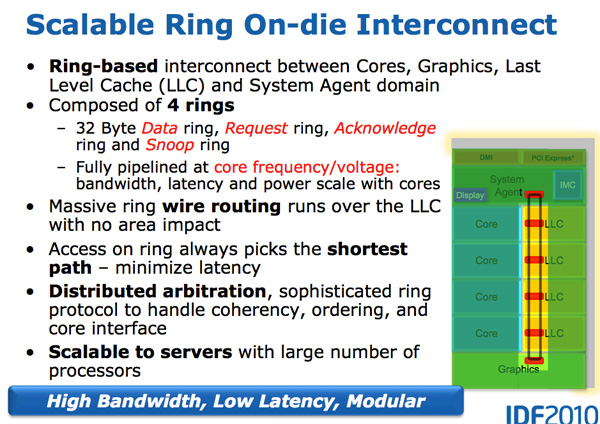
Architecturally, this is the same ring bus used in Nehalem EX and Westmere EX. Each core, each slice of L3 (LLC) cache, the on-die GPU, media engine and the system agent (fancy word for North Bridge) all have a stop on the ring bus. The bus is made up of four independent rings: a data ring, request ring, acknowledge ring and snoop ring. Each stop for each ring can accept 32-bytes of data per clock. As you increase core count and cache size, your cache bandwidth increases accordingly.
Per core you get the same amount of L3 cache bandwidth as in high end Westmere parts - 96GB/s. Aggregate bandwidth is 4x that in a quad-core system since you get a ring stop per core (384GB/s).
This means that L3 latency is significantly reduced from around 36 cycles in Westmere to 26 - 31 cycles in Sandy Bridge, with some variable cache latency as it depends on what core is accessing what slice of cache. Also unlike Westmere, the L3 cache now runs at the core clock speed - the concept of the un-core still exists but Intel calls it the “system agent” instead and it no longer includes the L3 cache. (The term ‘un-core’ is still in use today to describe interconnects.)
With the L3 cache running at the core clock you get the benefit of a much faster cache. The downside is the L3 underclocks itself in tandem with the processor cores as turbo and idle modes come into play. If the GPU needs the L3 while the CPUs are downclocked, the L3 cache won’t be running as fast as it could had it been independent, or the system has to power on the core and consume extra power.
The L3 cache is divided into slices, one associated with each core. As Sandy Bridge has a fully accessible L3 cache, each core can address the entire cache. Each slice gets its own stop and each slice has a full cache pipeline. In Westmere there was a single cache pipeline and queue that all cores forwarded requests to, but in Sandy Bridge it’s distributed per cache slice. The use of ring wire routing means that there is no big die area impact as more stops are added to the ring. Despite each of the consumers/producers on the ring get their own stop, the ring always takes the shortest path. Bus arbitration is distributed on the ring, each stop knows if there’s an empty slot on the ring one clock before.
The System Agent
For some reason Intel stopped using the term un-core in SB, and for Sandy Bridge it’s called the System Agent. (Again, un-core is now back in vogue for interconnects, IO, and memory controllers). The System Agent houses the traditional North Bridge. You get 16 PCIe 2.0 lanes that can be split into two x8s. There’s a redesigned dual-channel DDR3 memory controller that finally restores memory latency to around Lynnfield levels (Clarkdale moved the memory controller off the CPU die and onto the GPU).
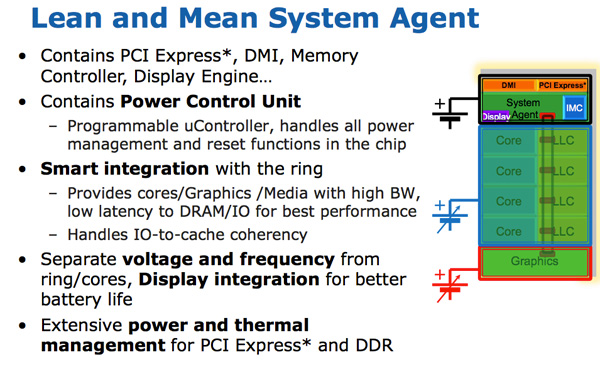
The SA also has the DMI interface, display engine and the PCU (Power Control Unit). The SA clock speed is lower than the rest of the core and it is on its own power plane.
Sandy Bridge Graphics
Another large performance improvement on Sandy Bridge vs. Westmere is in the graphics. While the CPU cores show a 10 - 30% improvement in performance, Sandy Bridge graphics performance is easily double what Intel delivered with pre-Westmere (Clarkdale/Arrandale). Despite the jump from 45nm to 32nm, SNB graphics improves through a significant increase in IPC.
The Sandy Bridge GPU is on-die built out of the same 32nm transistors as the CPU cores. The GPU is on its own power island and clock domain. The GPU can be powered down or clocked up independently of the CPU. Graphics turbo is available on both desktop and mobile parts, and you get more graphics turbo on Sandy Bridge.
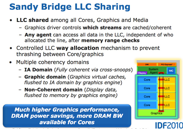
The GPU is treated like an equal citizen in the Sandy Bridge world, it gets equal access to the L3 cache. The graphics driver controls what gets into the L3 cache and you can even limit how much cache the GPU is able to use. Storing graphics data in the cache is particularly important as it saves trips to main memory which are costly from both a performance and power standpoint. Redesigning a GPU to make use of a cache isn’t a simple task.
SNB graphics (internally referred to as Gen 6 graphics) makes extensive use of fixed function hardware. The design mentality was anything that could be described by a fixed function should be implemented in fixed function hardware. The benefit is performance/power/die area efficiency, at the expense of flexibility.
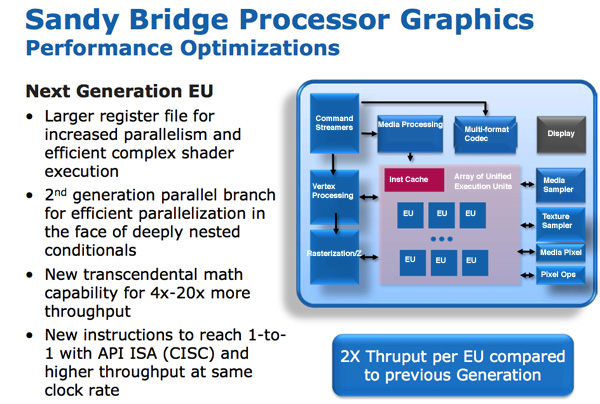
The programmable shader hardware is composed of shaders/cores/execution units that Intel calls EUs. Each EU can dual issue picking instructions from multiple threads. The internal ISA maps one-to-one with most DirectX 10 API instructions resulting in a very CISC-like architecture. Moving to one-to-one API to instruction mapping increases IPC by effectively increasing the width of the EUs.
There are other improvements within the EU. Transcendental math is handled by hardware in the EU and its performance has been sped up considerably. Intel told us that sine and cosine operations are several orders of magnitude faster now than they were in pre-Westmere graphics.
In previous Intel graphics architectures, the register file was repartitioned on the fly. If a thread needed fewer registers, the remaining registers could be allocated to another thread. While this was a great approach for saving die area, it proved to be a limiter for performance. In many cases threads couldn’t be worked on as there were no registers available for use. Intel moved from 64 to 80 registers per thread and finally to 120 for Sandy Bridge. The register count limiting thread count scenarios were alleviated.
At the time, all of these enhancements resulted in 2x the instruction throughput per EU.

Sandy Bridge vs. NVIDIA GeForce 310M Playing Starcraft 2
At launch there were two versions of Sandy Bridge graphics: one with 6 EUs and one with 12 EUs. All mobile parts (at launch) will use 12 EUs, while desktop SKUs may either use 6 or 12 depending on the model. Sandy Bridge was a step in the right direction for Intel, where integrated graphics were starting to become a requirement in anything consumer related, and Intel would slowly start to push the percentage of die area dedicated to GPU. Modern day equivalent desktop processors (2019) have 24 EUs (Gen 9.5), while future 10nm CPUs will have ~64 EUs (Gen11).
Sandy Bridge Media Engine
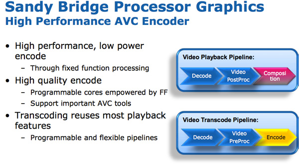
Sitting alongside the GPU is Sandy Bridge’s Media processor. Media processing in SNB is composed of two major components: video decode, and video encode.
The hardware accelerated decode engine is improved from the current generation: the entire video pipeline is now decoded via fixed function units. This is contrast to Intel’s pre-SNB design that uses the EU array for some video decode stages. As a result, Intel claims that SNB processor power is cut in half for HD video playback.
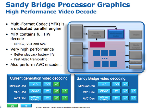
The video encode engine was a brand new addition to Sandy Bridge. Intel took a ~3 minute 1080p 30Mbps source video and transcoded it to a 640 x 360 iPhone video format. The total process took 14 seconds and completed at a rate of roughly 400 frames per second.
The fixed function encode/decode mentality is now pervasive in any graphics hardware for desktops and even smartphones. At the time, Sandy Bridge was using 3mm2 of the die for this basic encode/decode structure.
New, More Aggressive Turbo
Lynnfield was the first Intel CPU to aggressively pursue the idea of dynamically increasing the core clock of active CPU cores while powering down idle cores. The idea is that if you have a 95W TDP for a quad-core CPU, but three of those four cores are idle, then you can increase the clock speed of the one active core until you hit a turbo limit.
In all current generation processors the assumption is that the CPU reaches a turbo power limit immediately upon enabling turbo. In reality however, the CPU doesn’t heat up immediately - there’s a period of time where the CPU isn’t dissipating its full power consumption - there’s a ramp.
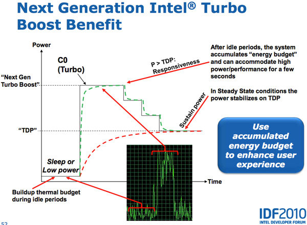
Sandy Bridge takes advantage of this by allowing the PCU to turbo up active cores above TDP for short periods of time (up to 25 seconds). The PCU keeps track of available thermal budget while idle and spends it when CPU demand goes up. The longer the CPU remains idle, the more potential it has to ramp up above TDP later on. When a workload comes around, the CPU can turbo above its TDP and step down as the processor heats up, eventually settling down at its TDP. While SNB can turbo up beyond its TDP, the PCU won’t allow the chip to exceed any reliability limits.
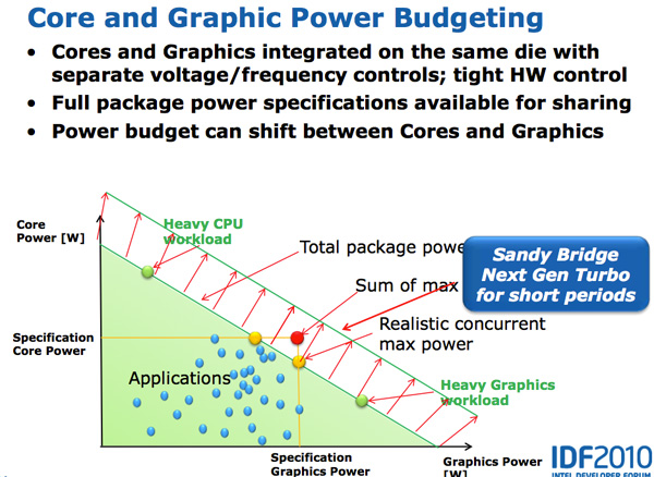
Both CPU and GPU turbo can work in tandem. Workloads that are more GPU bound running on SNB can result in the CPU cores clocking down and the GPU clocking up, while CPU bound tasks can drop the GPU frequency and increase CPU frequency. Sandy Bridge as a whole was a much more dynamic of a beast than anything that’s come before it.


213 Comments
View All Comments
monglerbongler - Friday, June 14, 2019 - link
You don't need to buy a new computer every year and with an intelligently made upfront investment you can potentially keep your desktop, with minimal or zero hardware upgrades, for a *very* long time/news at 11
If there is any argument that supports this its Intel's consumer/prosumer HEDT platforms.
The X99 was compelling over X58. The x299 is not even remotely compelling. I still have my old X99/ i7-5930k (6 core 40 lane PCIe3). its still fantastic, but thats at least partially because I bit the bullet and invested in a good motherboard and GPU at the time. All modern games still play fantastically and it can handle absolutely anything I throw at it.
More a statement of "future proofing" than inherent performance.
Sancus - Saturday, June 15, 2019 - link
It's always disappointing to see heavily GPU bottlenecked benchmarks in articles like these, without a clear warning that they are totally irrelevant to the question at hand.It also feeds into the false narrative that what resolution you play at matters for CPU benchmarks. What matters a lot more is what GAME you're playing, and these tests never benchmark the actually CPU bound multiplayer games that people are playing, because benchmarking those is Hard.
BlueB - Friday, June 21, 2019 - link
So if you're a gamer, there is STILL no reason for you to upgrade.Hogan773 - Friday, July 12, 2019 - link
I have a 2600K system with ASRock moboNow that there is so much hype about the Ryzen 3, is that my best option if I wanted to upgrade? I guess I would need a new mobo and memory in addition to the CPU. Otherwise I can use the same SSD etc.
tshoobs - Wednesday, July 17, 2019 - link
Still running my 3770 at stock clocks - "not a worry in the world, cold beer in my hand".Added an SSD and upgraded to a 1070 from the original GPU, . Best machine I've ever had.
gamefoo21 - Saturday, August 10, 2019 - link
I was running my X1950XT AIW at wonder level overclocks with a Pentium M overclocked, and crushing Athlon 64 users.It would have been really interesting to see that 7700K with DDR3. I run my 7700K @ 5Ghz with DDR3-2100 CL10 on a GA-Z170-HD3. Sadly the power delivery system on my board is at it's limits. :-(
But still a massive upgrade from a FX-8320e and MSI 970 mobo that I had before.
gamefoo21 - Saturday, August 10, 2019 - link
I forgot to add that it's 32GB(8GB x 4) G.Skill CL9 1866 1.5V that runs at 2100 CL10 at 1.5V but I have to give up 1T command rate.The GPU that I carried over is the Fury X. Bios modded of course so it's undervolted, underclocked and the HBM timings tightened. Whips the stock config.
The GPU is next up for upgrading, but I'm holding out for Navi with hardware RT and hopefully HBM. Once you get a taste of the low latency it's hard to go back.
OpenCL memory bandwidth for my Fury X punches over 320GB/s with single digit latency. The iGPU in my 7700K, is around 12-14GB/s and the latency is... -_-
BuffyCombs - Thursday, February 13, 2020 - link
There are several things about this article I dont like1. In the Game Tests, i actually dont care if one CPU is 50 Percent better when one shows 10 FPS and the other 15. Also I don’t care if it is 200 or 300 fps. So I would change to scale into a simple metric and that is: is it fun to play or not.
2. Development is not mentioned: The Core Wars has just started and the monopoly of intel is over. Why should we invest in new processors when competition has just begun. I predict price per performance will fall faster in the next years than it did in the previous 10 years. So buying now is buying into an overpriced and fast developing marked.
3. There is no Discussion if one should buy a used 2600k system today. I bought one a few weeks ago. It was 170 USD, has 16 GB of Ram and a gtx760. It plays all the games I throw at it and does the encoding of some videos I take in classes every week. Also I modified its cooler so that it runs very very silent. Using this system is a dream! Of course one could invest several times as much for a new system that is twice as fast in benchmarks but for now id rather save a few hundred bucks and invest when the competition becomes stagnant again or when some software I use really demands for it because of new instructions.
scrubman - Tuesday, March 23, 2021 - link
Great write-up! Love my 2600k still to this day and solid at 4.6GHz on air the whole time! I do see an upgrade this year though. She's been a beast!! Never thought the 300A Celeron OC to 450 would get beat! hahaSirBlot - Monday, July 25, 2022 - link
I get 60fps SotTR cpu game and render with rtx 3060ti with ray tracing on medium and everything else ultra. 2600k @4.2