Arm Announces Neoverse N1 & E1 Platforms & CPUs: Enabling A Huge Jump In Infrastructure Performance
by Andrei Frumusanu on February 20, 2019 9:00 AM ESTN1 Hyperscale Reference Design
A big part of what is defining the N1 Platform as an actual platform, is the fact that Arm is offering a full reference design with a set of IPs that is fully validated by Arm themselves.
Here we see three reference designs, a Neoverse N1 hyperscale design, which we’ll get into more detail shortly, an N1 edge design, and a Neoverse E1 edge design. Arm’s goals with the reference designs is to give vendors “sweet-spot” configuration options that they will then be able to implement with (relatively) minimal effort.
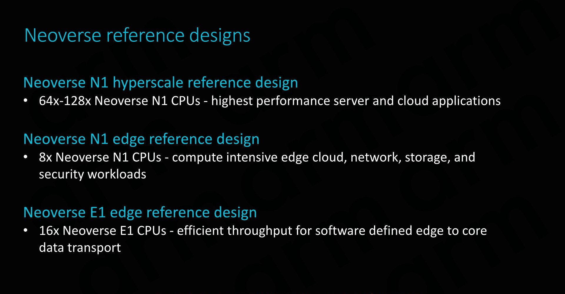
The N1 hyperscale design is what we’ll be covering in more detail as this represents Arm’s most cutting-edge and competitive product.
As covered on the previous page, at the heart we find the Neoverse N1 CPU in either 64 or 128 core configurations, integrated in a CMN-600 mesh network with either 64 or 128MB of SLC cache. We also see 128 lanes for PCIe 4 respectively CCIX interfaces which provide plenty of I/O bandwidth.
In terms of memory controllers, Arm employs 8x DD4 interfaces up to 3200MHz. Arm actually has abandoned development of its own memory controllers as customers in most cases opted for their own in-house designs or rather opted to choose IP from other third-party vendors such as Cadence or Synopsys. For the current reference designs Arm’s own DMC-520 was still up-to-date and a well-understood block for the company, although in the future newer memory controllers such as for DDR5 will have to rely on third-party IP. Naturally, the reference design targets the latest 7nm process node.

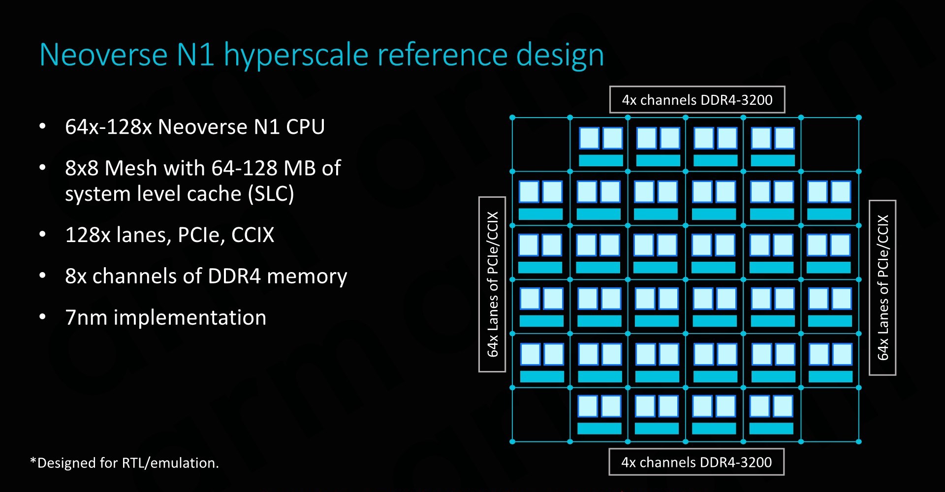
The physical implementation of the SoC would use replicable hierarchical building blocks for ease of design. A “CPU Tile” consists of the two N1 CPU cores, a slice/bank of the SLC cache as well as part of the CMN’s cross points and home-nodes. This CPU Tile is replicated to generate a “Super Tile”, what is added here is peripheral parts of the SoC such as I/O as well as memory controllers. Finally, replicating the super tile in flipped and mirrored implementations results in the final top-level mesh that is to be implemented on the SoC.
Scaling the design to 128 cores doesn’t represent an issue for the IP, although we’ll be hitting some practical limits in terms of current generation technology. Arm’s 64 core N1 reference design with 64MB of cache on a 7nm process node would result in a die size a little under 400mm², which probably is on the higher end of what vendors would want to target in terms of manufacturability. To alleviate such concerns, Arm also took a page out of AMD’s book and floated the idea of chiplet designs, where each chiplet would communicate over CCIX links. Inherently it’s up to the vendor to decide how they’ll want to design their solution, and Arm provides the essential building blocks and flexibility to enable this.
SmartNIC integration capability is also an important aspect of the design and its flexibility. To maximise compute capacity in large scale system, having accelerated network connectivity is key in actually achieving high throughput in the densest (and efficient) form-factor possible.
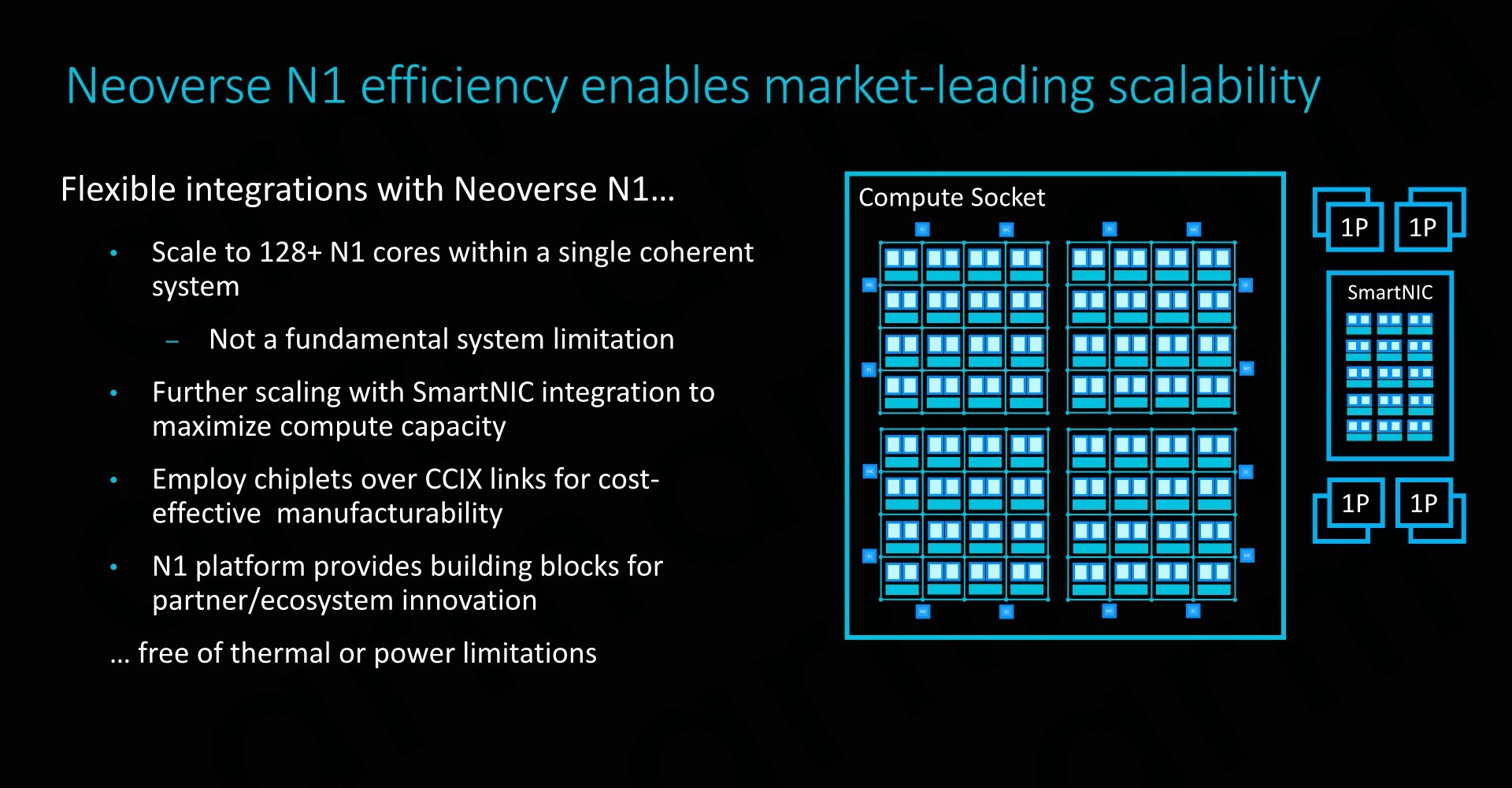
The CMN-600 allows for slave ports on its crosspoints: Here we can see MMUs connected with high bandwidth interfaces of up to 128GB/s. Attaching fixed-function hardware offloading IP thus would be extremely easy to implement.
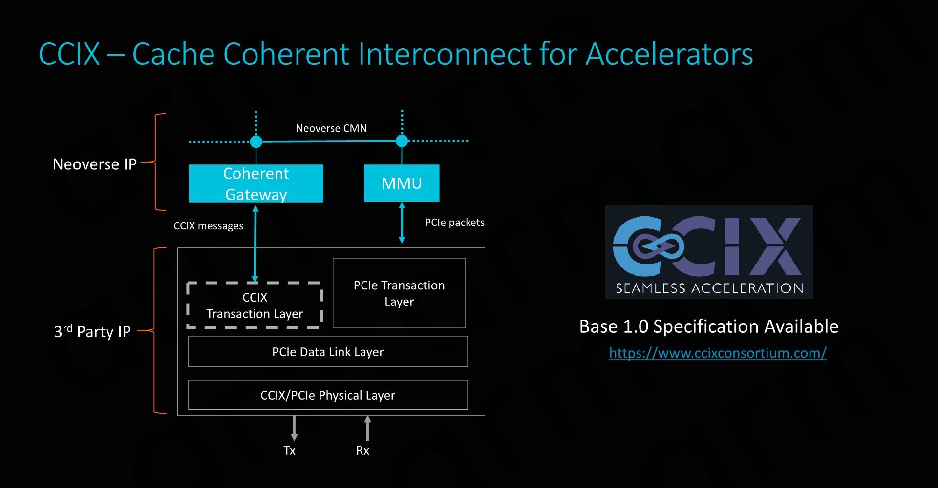
CCIX is extremely important for Arm as it enables its product portfolio to integrate with third-party IP offerings. Enabling cache coherency for external IP blocks is an incredibly attractive feature to have as it massively simplifies software design for the vendors. Essentially what this means is that software simply sees a single huge block of memory, whereas non-coherent systems require drivers and software to be aware and track what part of memory is valid and what isn’t. In terms of IP integration, Arm provides the CCIX coherent gateway that integrates with the CMN-600, while on the other side it’s the onus of the third-party IP provider to provide the CCIX translation layer.
Currently Xilinx will be among the first vendors to offer CCIX-enabled end-products in Q3 2019. With AMD also fully embracing CCIX, there’s some very exciting future potential for third-party accelerator hardware, and we be seeing new use-cases that just weren’t feasible before.
Power/Performance management
While it’s a bit weird to talk about power management in the context of implementation scalability (The average reader might think of it as a thermal/cooling consideration), there’s some very interesting implications in terms of how Arm simplifies the work needed to be done by the vendor.
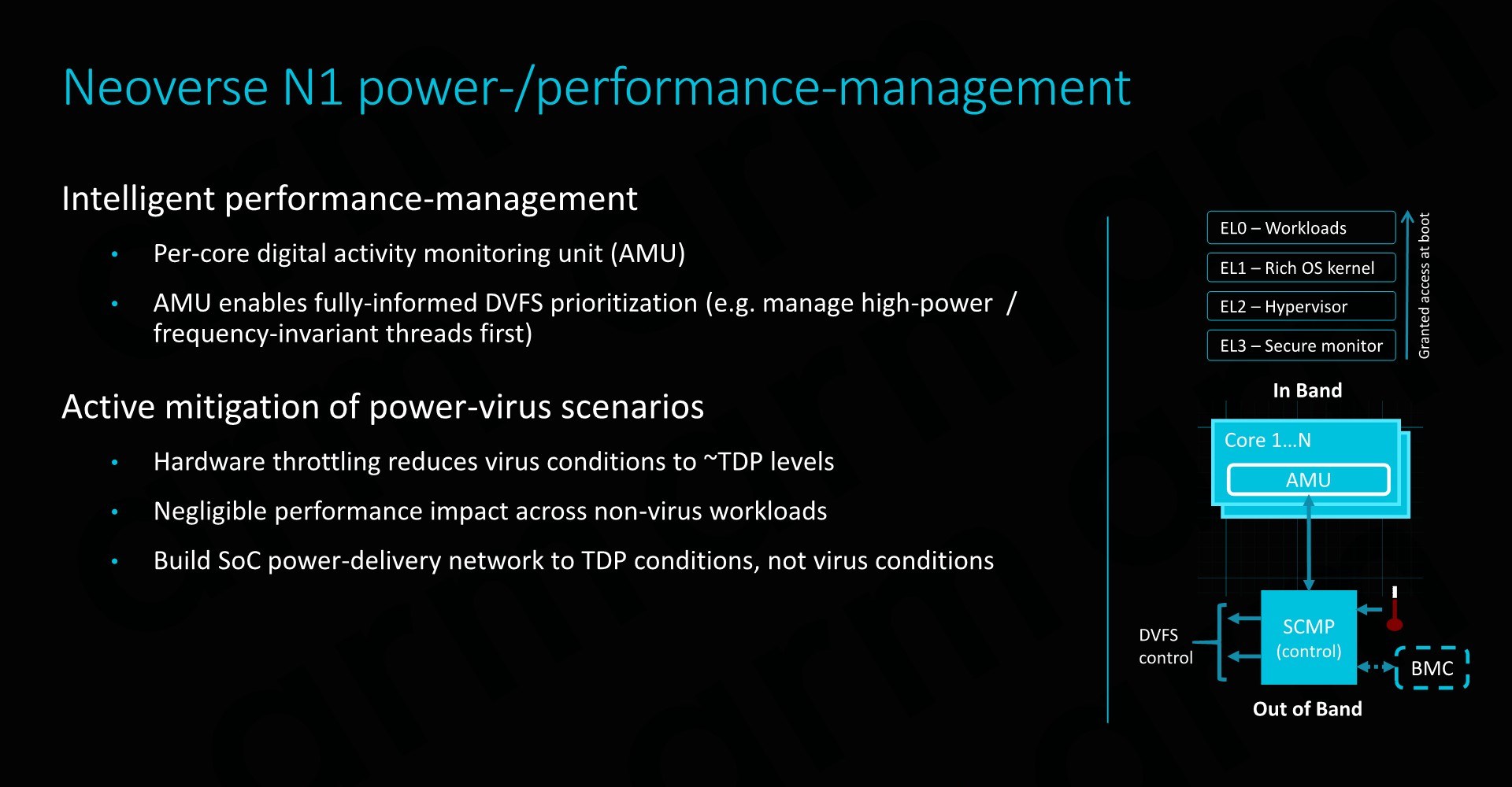
Along a chip’s logical design, a vendor must also implement a power delivery network that will be able to adequately support the IP. In real-world use-cases this means that the PDN needs to be as robust as to deal with the worst-case power scenario of a component. This is actually quite a headache for many vendors as the design requires complex models and in most cases the PDN will need to be over-engineered in order to offer guarantees of stability, which in turn raises the complexity and cost of the implementation.
Arm seeks to alleviate these concerns by offering extremely fine-grained DVFS mechanisms in the form of a dedicated micro-controller. The controller access detailed activity monitoring units inside the CPU cores, seeing what actual blocks and how many transistors are actually actively switching, and feeding this information back to the system controller to change DVFS states. This provides a certain level of hard-guarantee as to when the CPU enters power-virus-like workloads which can cause current spikes, and avoid them in time. This enables vendors to design their PDNs to more conservative tolerances, saving on implementation cost.


101 Comments
View All Comments
Santoval - Thursday, February 21, 2019 - link
"Both Intel and AMD have been making chips that take the CISC instructions and run them through an instruction decoder that then hands RISC instructions to the actual cpu."The instruction decoder is also part of an "actual CPU". Beside the decoder the front-end also has instruction fetch, a branch predictor, predecode (potentially), μOP & L1 instruction cache, instruction queues, a TLB, allocation queues etc etc All these units are most certainly parts of the "actual CPU".
I believe you rather meant "hands RISC-like instructions to the *back-end* of the CPU".
FunBunny2 - Thursday, February 21, 2019 - link
"The speed advantages on paper between RISC and CISC are in theory a wash. "not to keep beating the dead horse 360, dated as it is, but with the hardware of the time (and IBM was the top of the heap, then) the 360/30 ran the instruction set in micro-code. allegedly the first computer to even have microcode. ran like drek compared to the all-hardware versions of the machine. the '30 real cpu was long reputed to be some DEC machine.
"cpu design quite a bit without being so closely tied to backwards compatibility."
lots of folks say that, but makes no sense to me. compilers target the instruction set, which only changes when Intel publishes 'extensions'. whether those instructions are executed in pure ISA hardware, or a rat running in a spinning wheel (RISC), makes no difference to the compiler writer.
the profiling explanation for microcode over pure ISA hardware makes the most sense.
Wilco1 - Wednesday, February 20, 2019 - link
The only misinformation is from you. RTL simulation is widely used in the industry and is quite accurate.Studies have shown CISC instructions don't do more than RISC instructions - partly because compilers avoid CISC instructions, partly because CISC instructions are slow. That's why RISC works. But I wouldn't expect you to understand this.
FunBunny2 - Thursday, February 21, 2019 - link
"Studies have shown CISC instructions don't do more than RISC instructions "at least in the z world (and predecessors), there were/are some (I don't remember the count) of 'COBOL assist' instructions which were/are quite complex and were introduced to reduce the amount of times the COBOL coders had to 'drop down to assembler'. whether that's still true, I can't say.
DigitalVideoProcessor - Thursday, February 21, 2019 - link
CISC vs. RISC is a debate about instruction decode philosophy and it has almost zero bearing on the performance of a system. CISC machines reduce everything to RISC like operations. Saying one does more than another in a given clock is misinformation.melgross - Thursday, February 21, 2019 - link
Those wars are long over. No modern chip is either pure CISC or RISC. Those are long gone.Calin - Thursday, February 21, 2019 - link
SPECint, SPECfp, ... are "work done tasks" - what your're referring to was "MIPS" (or millions of instructions per second). This performance metric has lost its charm since internally x86 processors no longer use x86 instructions but large bundles of microoperations that are done in parallel and can be interleaved (so two instructions that follow each other are broken into micro operations which are reordered, and might be finalized in a different order).Kevin G - Thursday, February 21, 2019 - link
The thing is that real distinction of CISC vs. RISC is lost in their similar implementations: pipelined OoO parallel execution engines. While CISC encoding may* permit more operations to be contained within a single instruction but at the cost of having to decode that instruction into an optimal arrangement given the hardware. The price paid is in power consumption and complexity which may impact factors like maximum clock speed. In the era of many core and power limitations, these attributes are the foundation for RISC to have an edge over legacy CISC designs. Not to say that RISC architectures can't leverage instruction decoding either: expanding out the fields for registers to account for the larger rename register space is a simple procedure.Once chips begin parallel execution, the CISC advantage of doing more per instruction really starts to fall apart. The raw amount of work being done per cycle approaches the common limit of just how much parallelism can be extracted by an inherently serial stream of instructions. Arguably CISC designs can hit this sooner in terms of raw instruction count as the instruction stream is _effectively_ compressed compared to RISC.
*The concept of fused-multiply add instructions was an early staple of RISC architectures. Technically it goes against the purest ideal but traditional RISC designs permitted the number of operands in their instruction formatting to pull this off so they took advantage of an easy performance boost. x86 didn't gain this capability until AVX2 a few years ago.
peevee - Tuesday, February 26, 2019 - link
"I think you are forgetting the very nature of RISC (Arm) vs CISC (x86) architectures"This distinction does not exist in practice for decades.
wumpus - Wednesday, February 20, 2019 - link
It also shows a result showing Zen roughly half the performance of Intel, something that implies a fairly contrived situation. FX8350 might have had half (or worse) than Intel, but Zen is another story.I'm guessing that this involves AVX256 (or higher) specifically optimized for Intel (note that going to AVX512 is only a modest increase since the clockrate is brutally lowered to compensate for the increased power load. Also note that Zen2 (EPYC2 and Ryzen3000) will include native AVX256 execution paths).