AMD Ryzen 3rd Gen 'Matisse' Coming Mid 2019: Eight Core Zen 2 with PCIe 4.0 on Desktop
by Ian Cutress on January 9, 2019 1:01 PM EST
Blink and you miss it: AMD's keynote address this year was a whirlwind of primetime announcements for the company. The message is clear: AMD is committing itself to 7nm as the future process node that will drive the company's innovations starting in 2019. The first consumer products on 7nm will be the Ryzen 3rd Generation Desktop processors, using Zen 2 cores, offering more than competitive performance against Intel's best hardware. Also on the docket is a return to high-end graphics performance, with AMD set to release a 7nm graphics card that can spar blow-for-blow with the competition at the $700 price barrier.
AMD at CES 2019
One of the odd things about AMD’s announcements this show has been the tale of two halves. Normally a company will push out single major press release with everything in it. This year AMD discussed its news around Ryzen-3000 series mobile parts and AMD Chromebooks just as the show started, and we were all confused if this was going to constitute what was in the keynote or not – it would seem odd, after all, for the company to pre-announce its keynote announcements. Luckily, AMD has plenty to announce, and it’s all pretty juicy.
First up, CPUs. AMD presented its next generation 7nm desktop CPU, which is the 3rd Generation Ryzen.
Attacking the Mainstream CPU Market: Toe to Toe with Core i9-9900K
Ignore everything you might have heard about what AMD’s future desktop CPU is going to be. Here are most of the details you need to know.
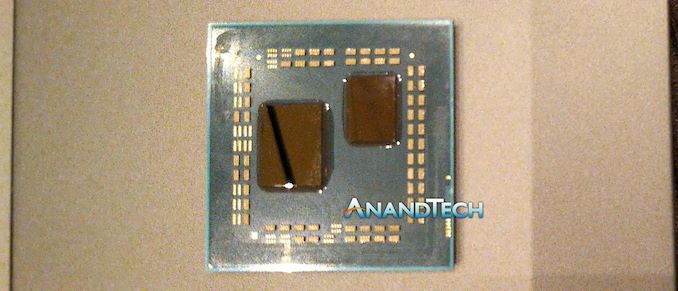
The new parts, codenamed Matisse, will be coming to market in mid-2019 (sometime in Q2 or Q3). The processor the company had on display was made from two pieces of silicon on the package: one eight-core 7nm chiplet made at TSMC, and a 14nm input/output chiplet with the dual memory controllers and the PCIe lanes, made at GlobalFoundries.
The company did state that it is the world’s first 7nm gaming CPU, and will also be the world’s first mainstream CPU to support PCIe 4.0 x16. At this time the company is not commenting on if the 3rd Gen is going to have a maximum of eight cores, or if this represents the best processor of the whole family.
Because the processor is still far away from launch, frequencies are not being finalized yet. However, the processor is for the AM4 socket, given that AMD has previously said that it intends to keep backwards compatibility for several generations. That will mean that this CPU will work in current 300 and 400-series AMD motherboards.
What this means for PCIe 4.0 is actually fairly simple. We expect there to be a new line of motherboards presumably something like X570 that will be PCIe 4.0 compatible, for any new PCIe 4.0 graphics cards that will be coming to market. One of the differences with PCIe 4.0 is that it can only handle PCB traces up to 7 inches before needing a redriver/retimer, so these extra ICs are needed for ports lower down the board. But, the first PCIe slot on most motherboards is in that limit, so it would appear that a lot of current 300 and 400 series motherboards, assuming the traces adhere to signal integrity specifications, could have their first PCIe slot rated at PCIe 4.0 with new firmware.
Going For Die Size
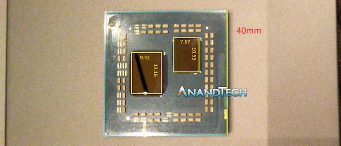
As we can see on the die shot above, the 8-core chiplet is smaller than the IO-die, similar to the 8+1 chiplet design on EPYC. The IO-die is not exactly one quarter of the EPYC IO-die, as I predicted might be the case back the Rome server processor announcement launch, but it is actually somewhere between one quarter and one half.
Doing some measurements on our imagery of the processor, and knowing that an AM4 processor is 40mm square, we measure the chiplet to be 10.53 x 7.67 mm = 80.80 mm2, whereas the IO die is 13.16mm x 9.32 mm = 122.63 mm2.
+15% Performance Generation on Generation, Minimum.
During the keynote, AMD showed some performance numbers using the new Ryzen 3rd Generation (Matisse) processor. The test in question was Cinebench R15.
Our internal numbers show the 2nd Generation Ryzen 7 2700X scores 1754.
This new 3rd Generation Ryzen processor scored 2023.
This would mean that at current non-final clocks, the new parts give a 15.3% increase in performance generation on generation. Cinebench is an idealized situation for AMD, but this is not at final clocks either. It will depend on the workload, but this is an interesting data point to have.
Identical Performance to the Core i9-9900K, Minimum.
Our internal benchmarks show the 9900K with a score of 2032.
The 8-core AMD processor scored 2023, and the Intel Core i9-9900K scored 2042.
Both systems were running on strong air cooling, and we were told that the Core i9-9900K was allowed to run at its standard frequencies on an ASUS motherboard. The AMD chip, by contrast, was not running at final clocks. AMD said that both systems had identical power supplies, DRAM, SSDs, operating systems, patches, and both with a Vega 64 graphics card.
At Just Over Half The Power…?!
Also, in that same test, it showed the system level power. This includes the motherboard, DRAM, SSD, and so on. As the systems were supposedly identical, this makes the comparison CPU only. The Intel system, during Cinebench, ran at 180W. This result is in line with what we’ve seen on our systems, and sounds correct. The AMD system on the other hand was running at 130-132W.
If we take a look at our average system idle power in our own reviews which is around 55W, this would make the Intel CPU around 125W, whereas the AMD CPU would be around 75W.
| AMD Benchmarks at CES 2019 | ||||||
| AnandTech | System Power | Idle Power* | Chip Power | CB 15 MT Score (pre-brief) |
CB 15 MT Score (on-stage) |
All-Core Frequency |
| AMD Zen 2 | 130W | 55W | 75W | 2023 | 2057 | ? |
| Intel i9-9900K | 180W | 55W | 125W | 2042 | 2040 | 4.7 GHz |
| *A rough estimate given our previous review testing | ||||||
This suggests that AMD’s new processors with the same amount of cores are offering performance parity in select benchmarks to Intel’s highest performing mainstream processor, while consuming a lot less power. Almost half as much power.
That is a powerful statement. (ed: pun not intended)
How has AMD done this? IPC or Frequency?
We know a few things about the new Zen 2 microarchitecture. We know it has an improved branch predictor unit, and improved prefetcher, better micro-op cache management, a larger micro-op cache, increased dispatch bandwidth, increased retire bandwidth, native support for 256-bit floating point math, double size FMA units, and double size load-store units. These last three parts are key elements to an FP-heavy benchmark like Cinebench, and work a lot in AMD’s favor.
As the Intel CPU was allowed to run as standard, even on the ASUS board, it should reach around 4.7 GHz on an all-core turbo. AMD’s frequencies on the processor were unknown; but also they are not final and we ‘should expect more’. Well, if the processor was only running at 75W, and they can push it another 20-30W, then there’s going to be more frequency and more performance to be had.
The one thing we don’t know is how well TSMC’s 7nm performs with respect to voltage and frequency. The only chips that currently exist on the process are smartphone chips that are under 3 GHz. There is no comparable metric – one would assume that in order to be competitive with the Core i9-9900K, the processor would have to match the all-core frequency (4.7 GHz) if it was at the same IPC.
If the CPU can't match IPC or frequency, then three things are possible:
- If the TSMC process can’t go that high on frequency, then AMD is ahead of Intel on IPC, which is a massive change in the ranks of modern x86 hardware.
- If the TSMC process can clock above 5.0 GHz, AND there is room to spare in the power budget to go even higher, then it’s going to be really funny seeing these processors complete.
- AMD's Hyperthreading for software such as CineBench is out of this world.
TL;DR = AMD’s 3rd Gen Ryzen Processors Are Another Step Up
When speaking with AMD, their representative said that there will be more information to follow as we get closer to launch. They’re happy for users to discuss whether it is IPC or frequency that is making AMD the winner here, and they’ll disclose more closer to the time.
Ian, I Thought You Predicted Two Chiplets?
Naturally, I assumed that AMD would be presenting a Ryzen-3000 series desktop processor with sixteen cores. For me, and a lot of others, felt like a natural progression, but here we are today with AMD only mentioning an eight core chip.
My money on two chiplets and a quarter IO die
— Ian Cutress (@IanCutress) November 7, 2018
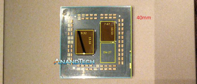
I predicted wrong, and I've lost my money (ed: in Las Vegas no less). But if we look at the processor, there’s still room for a surprise.
There’s room for a little something extra in there. There’s not much room for a little something extra, but I’m sure if AMD wanted to, there’s just enough space for another CPU chiplet (or a GPU chiplet) on this package. The question would then be around frequency and power, which are both valid.
There's also the question of lower core count processors and the cheaper end of the market. This processor uses silicon from TSMC, made in Taiwan, and GlobalFoundries, made in New York, then packaged together. We have heard some discussion from others not in the industry that this makes cheaper processors (sub $100) less feasible. It is entirely possible that AMD might address that market with future GPU.
What AMD has plans for in the future, I don’t know. I don’t have a crystal ball. But it does look like AMD has some room to grow in the future if they need to.


342 Comments
View All Comments
KOneJ - Wednesday, January 9, 2019 - link
And there's the limiting factor without HBM or some other memory architecture for on-package SoC-style iGPUs from AMD... bandwidth limitations. They're coming. People forget how Zen slides promised 5W TDP chips and GPU+CPU EPYC (IK about embedded...). It's all in the works, I'd guess.MrCommunistGen - Thursday, January 10, 2019 - link
In terms of functional units, RX 560 at 1024 Stream Processors across 16CUs isn't that much bigger than the 704 Stream Processors across 11CUs in a 2400G. With the shrink to 7nm power should come down nicely too.I think they have both the thermal and package-area budget for something in the range of 11 to 16 CUs. Maybe they'll build a 16CU GPU and only enable 14CUs to account for yields and keep power in check. That leaves room for enough of a GPU performance gain over the previous generation to be compelling.
As I'm sure others have said and will say, AMD is probably running up against the ceiling of what they can accomplish with on-package graphics without adding memory channels, moving to next gen DDR for the whole APU package, having on-package HBM, or adding a significant cache a la Crystal Well for Intel.
brakdoo - Wednesday, January 9, 2019 - link
The DRAM latency will always be bad. it's more important to have low cache latency but I'm not sure whether the L3$ or big L2$ are on the chiplet or the IO-chips...AlexDaum - Wednesday, January 9, 2019 - link
L1 and L2 are typically core local, so they will be on the chiplet for sure, and I am also pretty sure they put L3$ on the chiplet to, because the same chiplets are used on epyc and without a pretty big cache you could run into infinity fabric bandwidth problems for cache access from all chiplets.Maybe there is a second shared L3 or L4$ on the I/O hub? Some cache will be there for sure to buffer InfinityFabric and DRAM access, but they could put quite a big cache on there and use it as a L4$ victim cache, so that if 2 chiplets need the same data from DRAM that data is already in the I/O L4$ after the first read and you save the extra jump to DRAM. But that cache would be far less important on Ryzen where there is only one die
HStewart - Wednesday, January 9, 2019 - link
yes this is extremely surprising, in pre intel I series, this was the major advantage that AMD had over Intel. I hope for AMD stake this is a typo. Only thing I can think of it was more important to AMD to put the GPU on the chip then the memory control but ran in to difficulties putting memory controller on 7nm process.What comes to mind as solutions is Intel EMiB and similar - which allows different components of different die process on same die - even different manufactures like 8705g on my XPS 15 2in1
looncraz - Wednesday, January 9, 2019 - link
Point to point IFOP latency should be reasonably low. 5ns low. If the IMC is improved a little we might break even (or even improve) on latency.KOneJ - Wednesday, January 9, 2019 - link
Latency should be more linear and homogenized than Zen/Zen+ MCM designs. I don't see how near-latency isn't wrecked going out to main memory without sorting out far-latency, so there's got to be creative workarounds implemented there. I agree that Zen 2 DRAM latency may be better than some fear since clock domains, IF, the I/O die, and MCs may have more well-considered compromises than people have been accounting for. That opening on the package has got to be for a second die. Doesn't make sense otherwise. Minimizing trace-lengths, or maximizing heat dispersion would leave the layout bi-symmetrical or corner-to-corner. I'm just curious and confused why the I/O die for Matisse is so large compared to the features in Rome. Maybe it's for redundancy with yields... but 14nm yields were excellent and S/P Ridge didn't even utilize full PCIe lanes. I also doubt an L4 cache. Maybe this is necessary to maintain socket backwards-compatibility with both PCIe3 and PCIe4 on the I/O die? Only time will tell.looncraz - Saturday, January 12, 2019 - link
In order to service 16 cores I would expect SRAM to be present to buffer memory accesses. It might just be 2~4MiB, but it's pretty much going to be required.The die is a good 30mm^2 larger than needed, which is enough room for some L4, but we also don't know how large PCI-e 4.0 is nor the additional die space required for other features.
Given that Lisa Su verified the die is a unique die for Ryzen, it only makes sense that it doesn't have a bunch useless server bits on it like earlier models.
KOneJ - Saturday, January 12, 2019 - link
I could see a small L4, but not a large one. You're correct that it would conserve power and bandwidth by buffering memory accesses, but it's not necessary per se. I would've expected the Ryzen I/O die to be a bit smaller versus Rome's, so there's definitely that. Although Rome's need for L4 would be at least as great proportionally as Matisse's if needed so clearly at all. I don't think an L4 is likely, though it is possible. It may be an idea for a future Zen derivative as well. I'd say that's definitely something being considered if nothing else, but at what cost and how to implement effectively?looncraz - Tuesday, January 15, 2019 - link
There's potentially room for about 16MiB of L4, but that's making a LOT of assumptions about what else is on the die and the density of the L4 (just straight up using the L3 as a reference for 16MiB).The most valuable buffer could be a write coalescing buffer as it could keep the infinity fabric from backing up, thus allowing higher burst speeds. With four CCXes issuing writes at a potential rate of 50~100GB/s there will be a real need for a buffer to handle write bursts.