JEDEC Updates HBM Spec to Boost Capacity & Performance: 24 GB, 307 GB/s Per Stack
by Anton Shilov on December 19, 2018 6:15 PM EST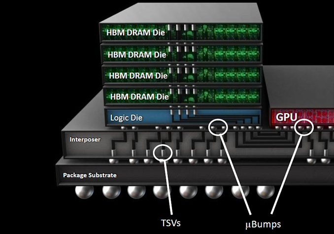
JEDEC this week published an updated version of its JESD235 specification, which describes HBM and HBM2 DRAM. The new version of the standard allows memory manufacturers to increase capacities of future HBM stacks to 24 GB and boost their bandwidth to 307 GB/s per stack.
On the capacity front, the new version of the specification, JESD235B, had added support for 12-Hi chip stacks. With 4 more layers than the previous limit of 8-Hi stacks, this will allow memory manufacturers to produce 12 GB stacks at current densities, and 24 GB stacks in the future when 16 Gb layers become available. Though it's worth noting that while 12-Hi stacks are now part of the HBM specification, the group still lists the physical dimensions of a 12-Hi KGSD (known good stacked die) as "TBD", so it's not immediately clear right now whether 12-Hi stacks will follow the same 720μm typical/745μm maximum stack height rules as the current 2/4/8-Hi configurations. Otherwise the configuration of the stacks themselves are unchanged; the new KGSDs will continue to feature up to eight 128-bit channels as well as a 1024-bit physical interface.
As for performance, the HBM standard now also supports data transfer rates of up to 2.4 Gbps per pin (i.e., 307 GB/s per stack), up from 2 Gbps supported by the JESD235A. It is noteworthy that Samsung’s Aquabolt and SK Hynix’s HBM2 memory chips already support 2.4 Gbps speeds at 1.2 V, so from actual performance point of view the new spec does not bring any significant changes. However this update does finally canonize the 2.4 Gbps data rate into the official standard, and meanwhile the new spec will enable other DRAM makers to release 2.4 Gbps products as well.
All told, the updated specification means that a fully built-out 4096-bit HBM memory subsystem following the JESD235B spec can now contain 96 GB of memory with a peak bandwidth of 1.228 TB/s.
Though it remains to be seen when makers of memory will be ready with their 12-Hi HBM memory chips. To date, no one has announced any 12-Hi products; however I wouldn't expect JEDEC to be adding even taller stacks to the standard unless someone was in the process of building said memory.
Related Reading:
- Samsung Starts Production of HBM2 “Aquabolt” Memory: 8 GB, 2.4 Gbps
- JEDEC Publishes HBM2 Specification as Samsung Begins Mass Production of Chips
- SK Hynix Adds HBM2 to Catalog: 4 GB Stacks Set to Be Available in Q3
Source: JEDEC


15 Comments
View All Comments
MajGenRelativity - Thursday, December 20, 2018 - link
96GB of HBM is indeed plenty for the vast majority of people, but the price of a CPU with 96GB of HBM is also above budget for the vast majority of people. Your L4 cache idea, similar to Crystalwell, would probably be a better bet for iGPUs or somesuch.sing_electric - Thursday, December 20, 2018 - link
"Intel/AMD" is ironically the right way to put it: Intel's Kaby Lake G processors with AMD's graphics on-package also include HBM2 memory, but for the graphics processor. Not what you asked for, but... well, close-ish?I've seen numbers that suggest that HBM2 is ~2-3x the cost of DDR4 for a given capacity, plus ~$25 for the interposer, so you'd probably be looking at $150 (minimum) to add 8GB on package, and a little less than ~$300 for 16GB. On top of that, you'd need a new socket and a low-volume, (therefore) high-cost motherboard. I really wonder if, when all's said and done, those costs would really be worth the extra performance over DDR4. In a given box, you could easily double the RAM and still save money, and for large installs, get substantially more servers for the same cash.
boeush - Thursday, December 20, 2018 - link
At some point, distance from CPU to RAM will become a big performance (and power) bottleneck. Branch prediction and speculative execution will only get you so far, particularly in these days of side-channel attacks and tight per-core power budgets that are made tighter by power-hungry interconnect fabrics. Meanwhile, ongoing process shrinks, and new transistor designs/materials, will continue ratcheting up the CPU frequencies, further raising the cost of pipeline stalls...Even if not going with HBM in particular, I can see package-on-package combos of CPU + RAM (with some TSV and/or interposer tech to tie it all together) increasingly becoming a necessity over the next few years. In multi-chiplet CPU/SoC designs that need an interposer anyway, upgrading the interposer to also handle on-package RAM (whether HBM or not) would likely not further raise the cost(s) all that much. And as far as HBM per-bit cost, I suspect it's more an issue of high-volume manufacturing and scale-up. Intrinsically, HBM requires far less packaging and auxiliary chips/circuitry, so should be fundamentally cheaper than DDR4+ RAM on a per-bit basis - if all other factors (such as supply chain scale) were equivalent. Plus, HBM is more power-efficient than DDR, which would allow more power to be allocated to processing, thus further boosting performance.
Over the next few years, I can see HBM completely replacing DDR on all consumer and prosumer-grade devices, with DDR eventually getting relegated to large servers and supercomputers as a "niche" technology. Of course, just because it's possible or even likely (IMHO), doesn't mean it will necessarily happen: ultimately, it's up to the long-term decisions and investments made by the market leaders.
iwod - Thursday, December 20, 2018 - link
I naturally assume in 7nm Top End GPU, there is going to be a need for higher bandwidth which needs either 512bit GDDR6 or HBM2?Which one will be cheaper? 512bit memory interface is expensive. When does the line cross and HBM2 becomes a better solution? Or are they still priced far apart?
integracija - Monday, December 31, 2018 - link
https://integracija.tumblr.com/