Intel's Architecture Day 2018: The Future of Core, Intel GPUs, 10nm, and Hybrid x86
by Dr. Ian Cutress on December 12, 2018 9:00 AM EST- Posted in
- CPUs
- Memory
- Intel
- GPUs
- DRAM
- Architecture
- Microarchitecture
- Xe
Changing How Chips are Made: 3D Packaging with FOVEROS
Anyone who has followed any amount of chip design in semiconductors should well-aware that most of the CPUs and SoCs in production today are based on monolithic dies – single pieces of silicon the have all what is needed inside, before being placed on a package and into a system. While rarer, there are multi-chip packages, were multiple chips go in one package with a shared connection. Beyond this we have seen interposers or embedded bridges designed to bring different chips together with high-speed interconnects. Now Intel is ready to bring 3D stacking into the mass market.
One of the biggest challenges in modern chip design is minimizing die area. A small die decreases costs – typically power too – and can make it easier to implement in a system. When it comes down to extracting performance however, we are at the limits of scale – one of the downsides of big monolithic dies, or even multi-chip packages, is that memory is too far away. Intel today is now ready to talk about its Foveros technology, which involves active interposers in small form factors to bring differentiated technologies together.
Foveros: It’s Greek for Awesome, Apparently
The way Raja introduced this technology started with discussing process technologies. Intel has for many years/decades been focused on high performance process nodes, trying to extract as much as possible from its high-performance cores. Alongside this, Intel also runs an IO optimized process node on a similar cadence but more suitable for PCH or SoC-type functions.
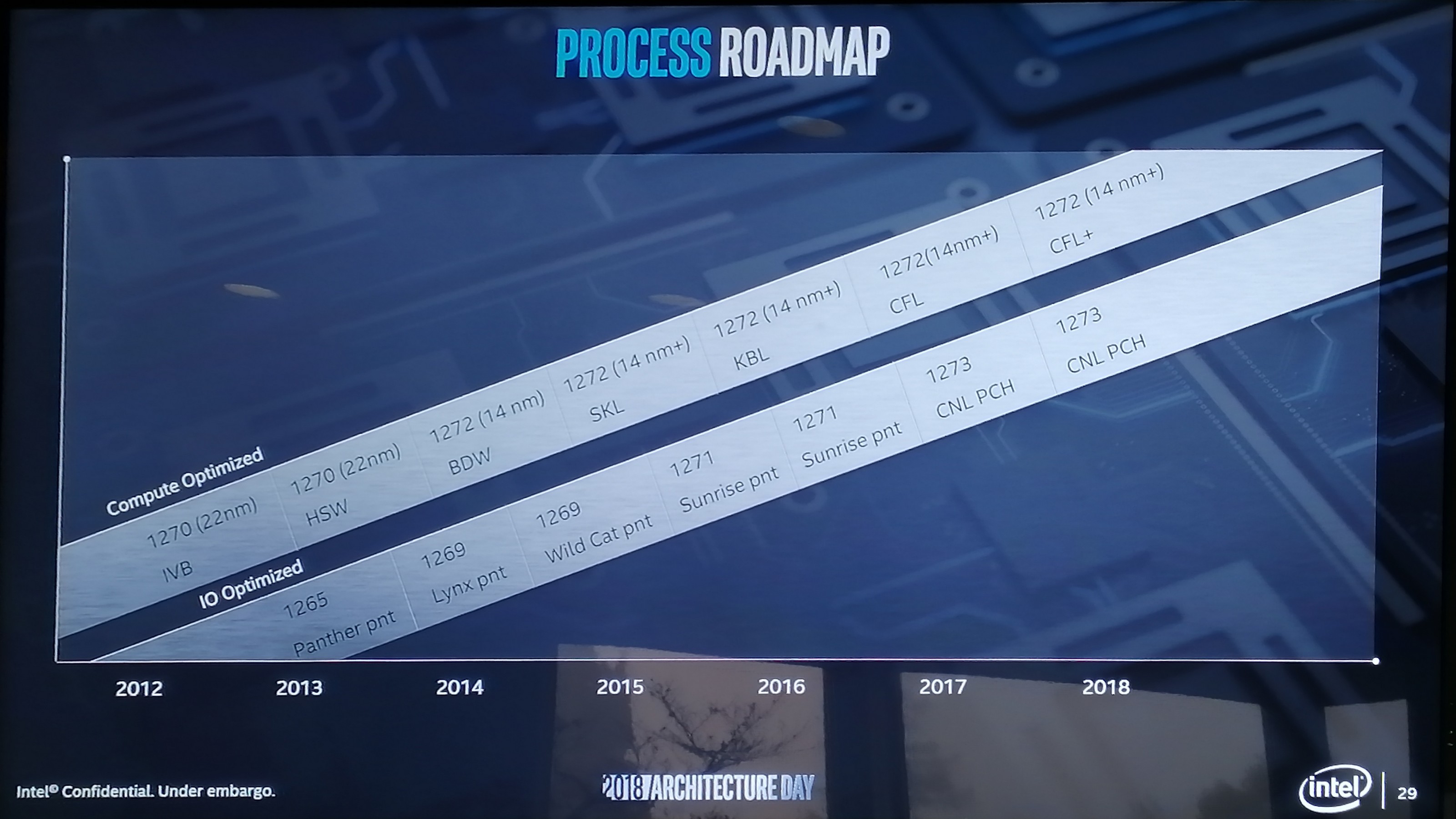
The 126x and 127x are the internal numbering systems for Intel’s process node technologies, although they don’t differentiate between BKM updates for the "+" node variants it turns out. But the point here is that Intel already knows that it needs certain process optimizations in place depending on the type of transistors, performance, and power needed. Going forward, Intel is going to be expanding its node base out so it can cover more power and performance points.
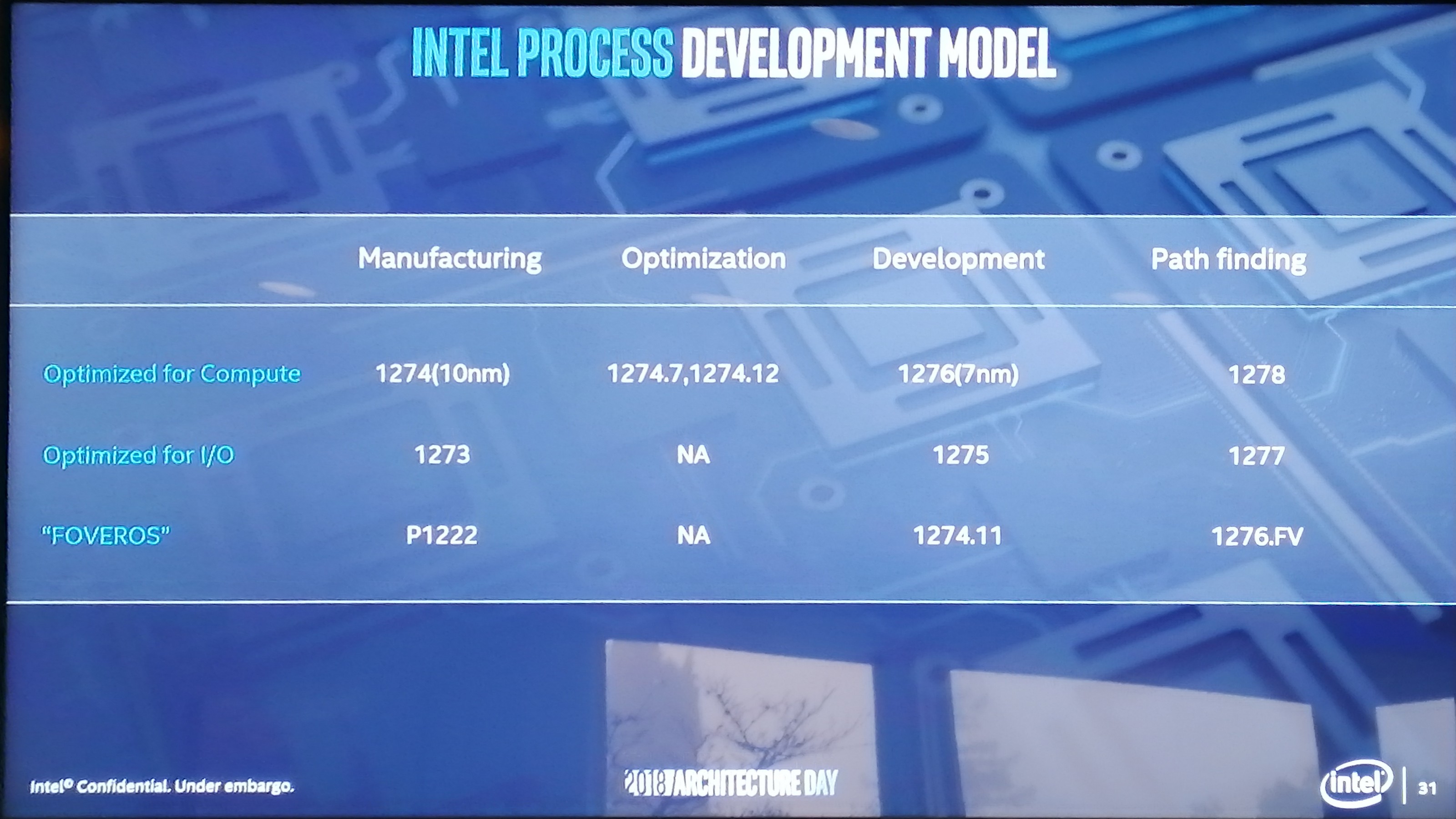
So for this example, Raja pulled out the current set of process technologies for 2019. For a manufacturing process, compute has the 1274 process on 10nm, IO has the 1273 process (14nm), while this new special Foveros technology is under P1222. Alongside the manufacturing, Intel will be working on optimizations focusing on the compute aspects of the manufacturing node. There will also be a set of developments for future node technologies, and the final column shows that Intel has path-finding research to look into future technologies and determine what capabilities will be possible on future designs. This sounds pretty much what a company like Intel should be doing, so no argument from me so far. The goal here is that each type of transistor use case can be different, and there isn’t a one-size fits all approach.

One way to assist with this is through chiplets and packaging. By picking the best transistor for the job in each case, whether it is CPU, GPU, IO, FPGA, RF, or anything else, with the correct packaging, it can be put together to get the best optimizations available.
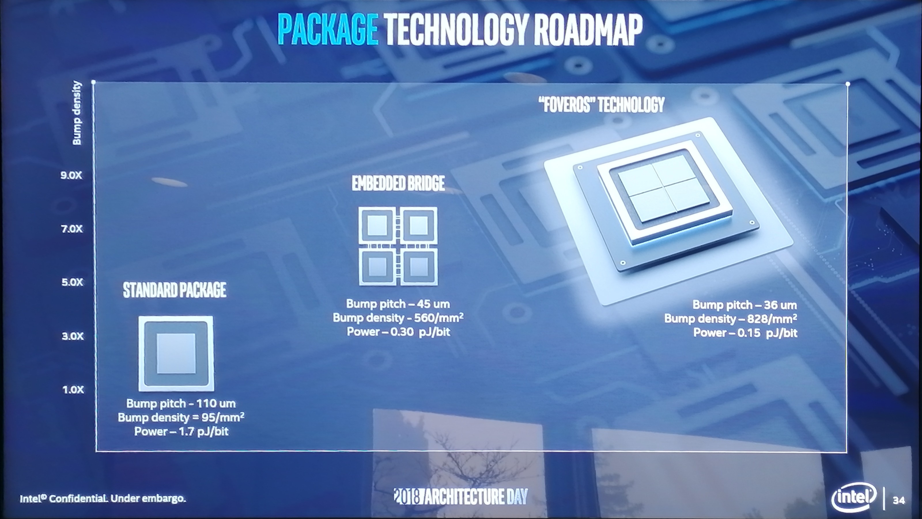
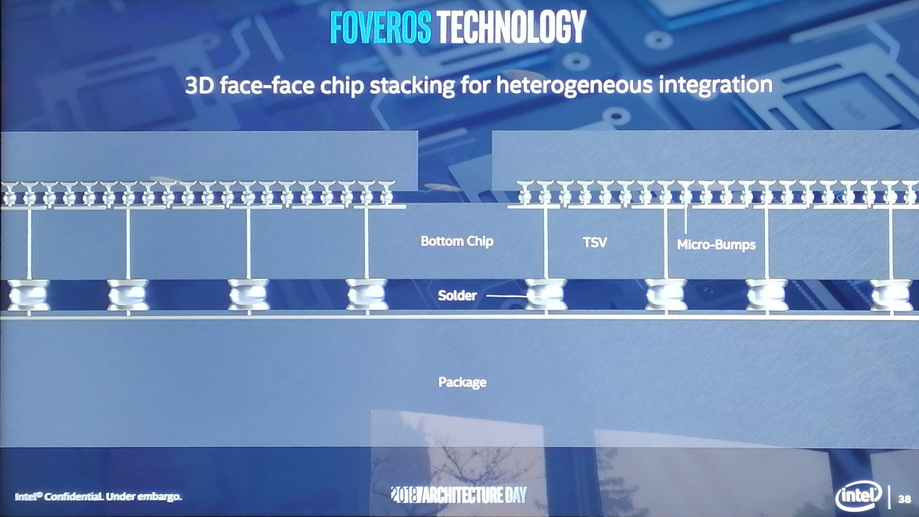
So here’s where Foveros fits in. Foveros is Intel’s new active interposer technology designed as a step above its own EMIB designs for small form-factor implementations, or those with extreme memory bandwidth requirements. For these designs the power per bit of data transferred is super low, however the packaging technology has to deal with the decreased bump pitch, the increased bump density, and also the chip stacking technology. Intel says that Foveros is ready for prime time, and they can produce it at scale.
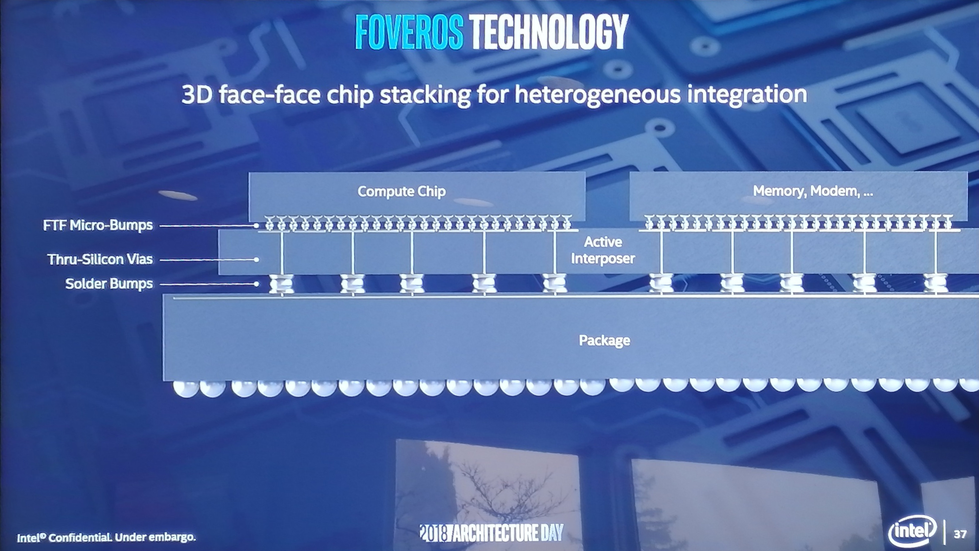
So this Foveros ‘3D’ packaging just sounds like a silicon interposer, such as what we’ve seen on AMD’s Fiji or NVIDIA’s high-end datacenter GPUs. However Intel is going above what those products are doing by actually making the interposer part of the design. The interposer contains the through-silicon vias and traces required to bring power and data to the chips on top, but the interposer also carries the PCH or IO of the platform. It is, in effect, a fully working PCH, but with vias to allow chips to be connected on top.
The first iteration of this technology is less complicated that the slide above, just using a set of CPU cores attached to the PCH below, but the idea is that a large interposer can have select functions on it and those can be removed from the chips above to save space. This also lets Intel use the different transistor types in different chips – the example we were given uses an interposer built on the 22FFL process node, with a 10nm set of CPUs on the top die. Above this, DRAM is provided in a POP package. Sounds cool, right?
In actual fact, Intel had a Foveros chip or two working in the demo area. These, Intel explained, were hybrid x86 designs that combined a single big Core with four smaller Atom cores on the same 10nm piece of silicon. I’m sure I’ve heard about big.Little before, but I was shocked that Intel is actually going to do it! We managed to take a photo of the block diagram, which Intel removed from its slide deck before sending it out to the press after the presentations. All details on the next page.


148 Comments
View All Comments
f1nalpr1m3 - Wednesday, December 12, 2018 - link
Yeah, they totally put it together in three weeks and everything.Get a clue.
pkgtech - Thursday, December 20, 2018 - link
For years Sohail Ahmed was the roadblock to Intel doing any creative package technology by blocking silicon support. He finally was shown for what he was after 2+ year process technology delays and re-invented this. Good riddance SohailAdonisds - Wednesday, December 12, 2018 - link
How do the Intel process delays influence their microarchitecture plans? 10 nm was already supposed to be here and with it its new microarchitecture, Ice Lake. Does the Ice Lake design continue to get improved as the delays kept happening or was it finalized years ago? Why? What about the microarchutectures succeeding Ice Lake?III-V - Wednesday, December 12, 2018 - link
This is Ice Lake. Might be a 14nm port (unclear at this point why the name change), but it's at the very least a close relative.III-V - Wednesday, December 12, 2018 - link
Actually, given the name on the heat sink, it is probably just straight up Ice LakeHStewart - Thursday, December 13, 2018 - link
I believe the road map states Ice Lake will be on 10nm. More importantly it will be on Sunny Cove which is significant update to Architexture.AdhesiveTeflon - Wednesday, December 12, 2018 - link
Intel and their naming scheme....they should call one "blue slushie lake"prisonerX - Wednesday, December 12, 2018 - link
Plans? Intel are in full scale panic mode right now. I'm sure they have new plans every week.jjj - Wednesday, December 12, 2018 - link
LOL you went in full fanboy mode with the 144mm package being small.The package is that size for PoP, the die is much much smaller, they can fit way more 10nm cores than that in such a large area, even without a base die.
Anyway, there are no relevant details on Foveros and that's problematic. The first question is cost, then you would want to know details about pitch and so on. Intel is by no means the first to announce such a solution so the details are what matters.
This is how you get to a 3D monolithic die in some years so any foundry that wants to stay in the most advanced node game, needs to push the packaging roadmap.
Ian Cutress - Wednesday, December 12, 2018 - link
I specifically said the package was small, and the die was smaller than the package.