Intel's Architecture Day 2018: The Future of Core, Intel GPUs, 10nm, and Hybrid x86
by Dr. Ian Cutress on December 12, 2018 9:00 AM EST- Posted in
- CPUs
- Memory
- Intel
- GPUs
- DRAM
- Architecture
- Microarchitecture
- Xe
Changing How Chips are Made: 3D Packaging with FOVEROS
Anyone who has followed any amount of chip design in semiconductors should well-aware that most of the CPUs and SoCs in production today are based on monolithic dies – single pieces of silicon the have all what is needed inside, before being placed on a package and into a system. While rarer, there are multi-chip packages, were multiple chips go in one package with a shared connection. Beyond this we have seen interposers or embedded bridges designed to bring different chips together with high-speed interconnects. Now Intel is ready to bring 3D stacking into the mass market.
One of the biggest challenges in modern chip design is minimizing die area. A small die decreases costs – typically power too – and can make it easier to implement in a system. When it comes down to extracting performance however, we are at the limits of scale – one of the downsides of big monolithic dies, or even multi-chip packages, is that memory is too far away. Intel today is now ready to talk about its Foveros technology, which involves active interposers in small form factors to bring differentiated technologies together.
Foveros: It’s Greek for Awesome, Apparently
The way Raja introduced this technology started with discussing process technologies. Intel has for many years/decades been focused on high performance process nodes, trying to extract as much as possible from its high-performance cores. Alongside this, Intel also runs an IO optimized process node on a similar cadence but more suitable for PCH or SoC-type functions.
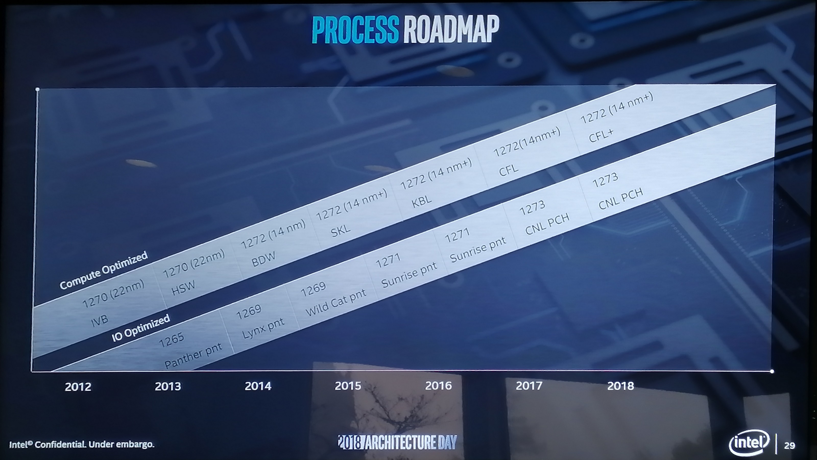
The 126x and 127x are the internal numbering systems for Intel’s process node technologies, although they don’t differentiate between BKM updates for the "+" node variants it turns out. But the point here is that Intel already knows that it needs certain process optimizations in place depending on the type of transistors, performance, and power needed. Going forward, Intel is going to be expanding its node base out so it can cover more power and performance points.
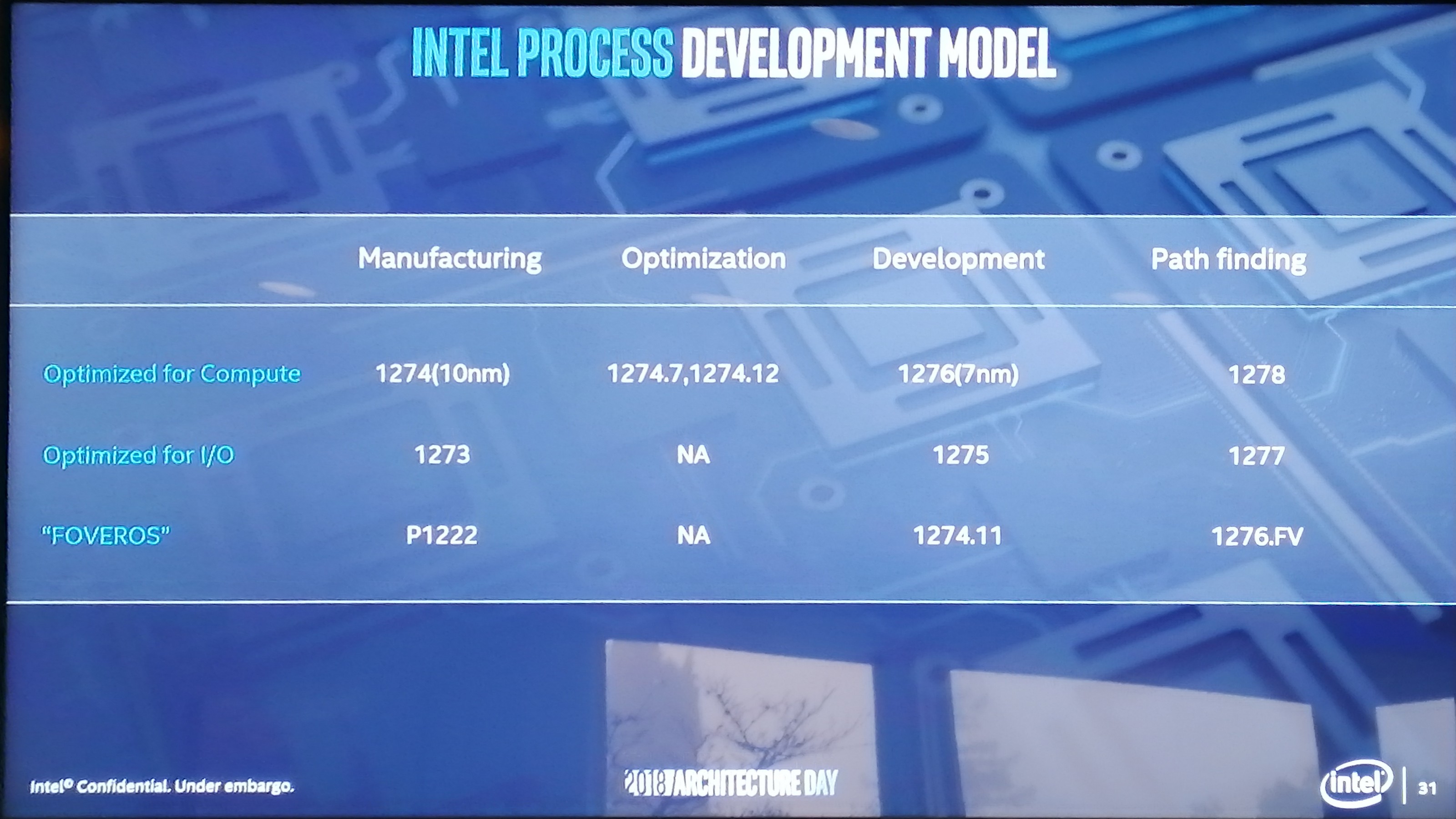
So for this example, Raja pulled out the current set of process technologies for 2019. For a manufacturing process, compute has the 1274 process on 10nm, IO has the 1273 process (14nm), while this new special Foveros technology is under P1222. Alongside the manufacturing, Intel will be working on optimizations focusing on the compute aspects of the manufacturing node. There will also be a set of developments for future node technologies, and the final column shows that Intel has path-finding research to look into future technologies and determine what capabilities will be possible on future designs. This sounds pretty much what a company like Intel should be doing, so no argument from me so far. The goal here is that each type of transistor use case can be different, and there isn’t a one-size fits all approach.

One way to assist with this is through chiplets and packaging. By picking the best transistor for the job in each case, whether it is CPU, GPU, IO, FPGA, RF, or anything else, with the correct packaging, it can be put together to get the best optimizations available.
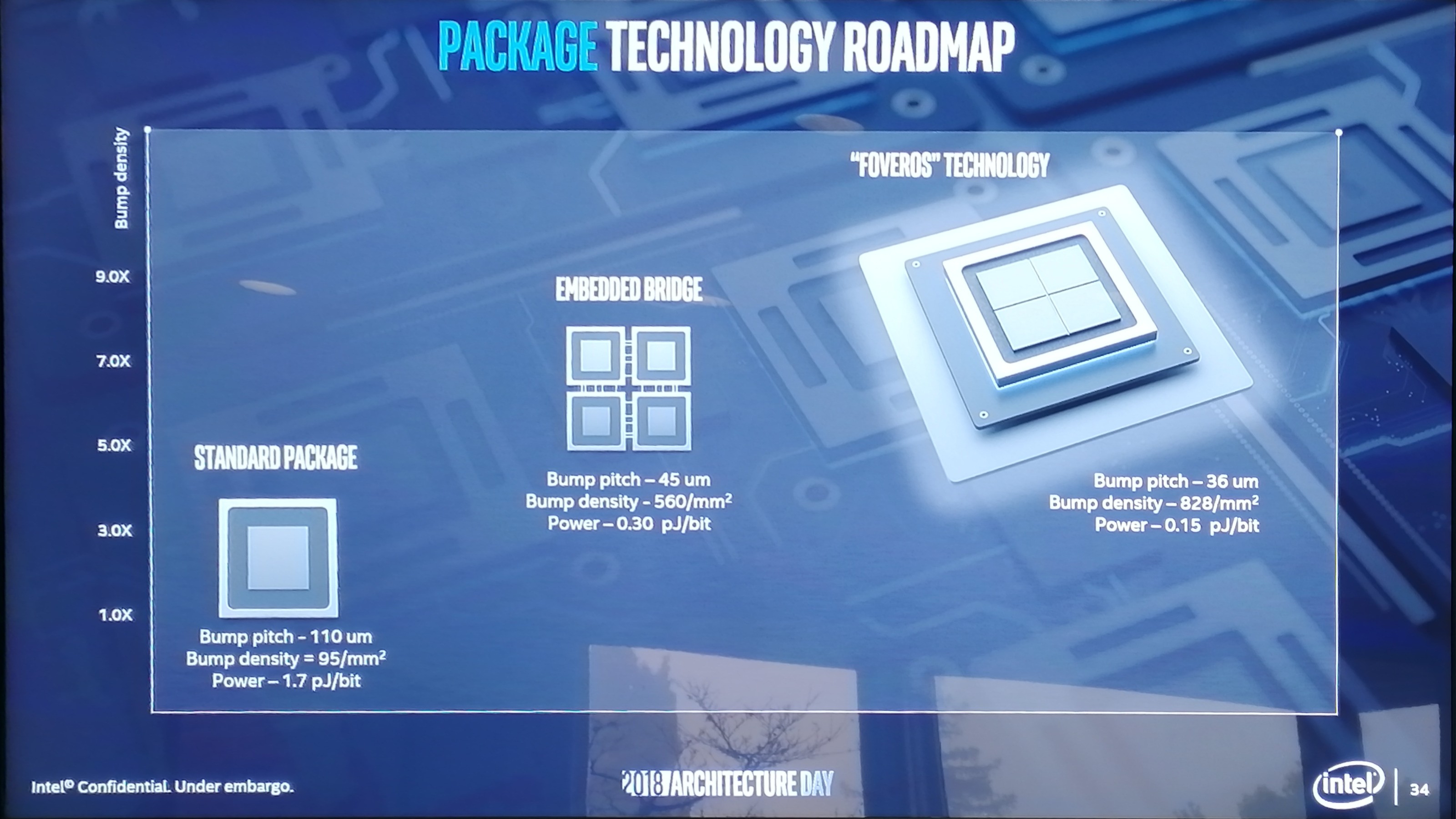
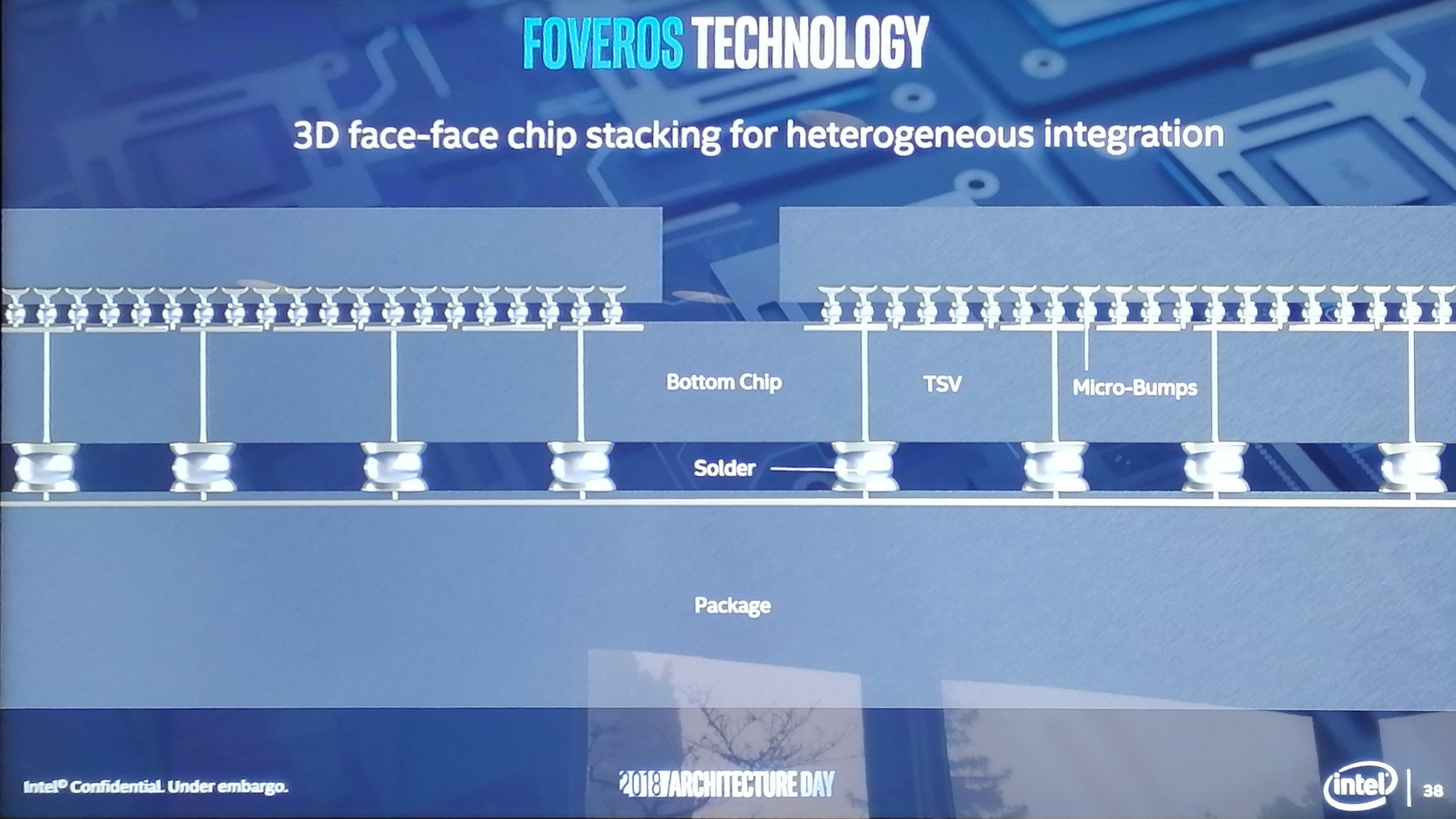
So here’s where Foveros fits in. Foveros is Intel’s new active interposer technology designed as a step above its own EMIB designs for small form-factor implementations, or those with extreme memory bandwidth requirements. For these designs the power per bit of data transferred is super low, however the packaging technology has to deal with the decreased bump pitch, the increased bump density, and also the chip stacking technology. Intel says that Foveros is ready for prime time, and they can produce it at scale.
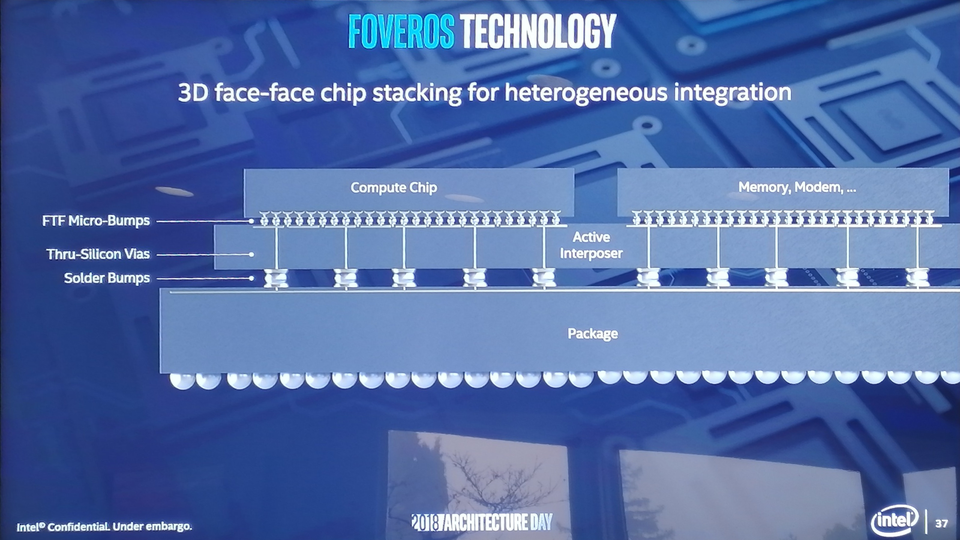
So this Foveros ‘3D’ packaging just sounds like a silicon interposer, such as what we’ve seen on AMD’s Fiji or NVIDIA’s high-end datacenter GPUs. However Intel is going above what those products are doing by actually making the interposer part of the design. The interposer contains the through-silicon vias and traces required to bring power and data to the chips on top, but the interposer also carries the PCH or IO of the platform. It is, in effect, a fully working PCH, but with vias to allow chips to be connected on top.
The first iteration of this technology is less complicated that the slide above, just using a set of CPU cores attached to the PCH below, but the idea is that a large interposer can have select functions on it and those can be removed from the chips above to save space. This also lets Intel use the different transistor types in different chips – the example we were given uses an interposer built on the 22FFL process node, with a 10nm set of CPUs on the top die. Above this, DRAM is provided in a POP package. Sounds cool, right?
In actual fact, Intel had a Foveros chip or two working in the demo area. These, Intel explained, were hybrid x86 designs that combined a single big Core with four smaller Atom cores on the same 10nm piece of silicon. I’m sure I’ve heard about big.Little before, but I was shocked that Intel is actually going to do it! We managed to take a photo of the block diagram, which Intel removed from its slide deck before sending it out to the press after the presentations. All details on the next page.


148 Comments
View All Comments
CajunArson - Wednesday, December 12, 2018 - link
There's nothing whatsoever revolutionary about "chiplets". A 10 year old core 2 quad used exactly the same technology that AMD calls "chiplets" in 2019 and AMD fantards like you even insulted the Core 2 quad for doing it.Maybe you should actually read the article about what a active interposer can do vs. wiring standard hunks of silicon to a PCB in literally the same way it was done in the 1970s before you run around acting like AMD is the only company to ever innovate anything.
sgeocla - Wednesday, December 12, 2018 - link
I've been reading articles about Intel 10nm promises for years now. And then we got failed laptop chips and low power pc boxes to appease 'mass production' status and not get sued by investors for false claims.Forgive me if I abstain my drooling until Intel actually delivers something that does not require industrial chillers. BTY where is that 28 core HEDT chips anyway ?
Targon - Wednesday, December 12, 2018 - link
There is always a point where the WHEN something is used sets a new direction. Multi-CPU in a workstation/server moving to a single processor with multiple cores was a big shift. Moving from two cores linked together when cache coherency was a big problem to a single dual-core without an interposer was a better way to go. It all comes down to if there is a performance boost or degradation as a result of the technology/implementation.With that said, a single CPU with 64 cores is fairly significant, and keeping the performance from being horrible with that many cores is the reason AMD has been praised. Price/performance for the server market and such.
For a long time, Intel was seen as the king when it came to clock speeds and performance, but Intel hasn't had a significant boost to IPC in over three years. Intel has also been promising 10nm for three years, and still no sign of it, with the promise of holidays 2019.
So, Intel still has nothing, they have vague promises of ways they will improve performance, but it remains to be seen if the performance will actually be better if 10nm slips again. On the flip side, AMD clearly has significant performance boosts from Ryzen 3rd generation in 2019(March/April being when many expect it). 7nm from AMD isn't a, "will they?" question, it isn't even a "when?", with CES in one month and with it, the answers. IPC improvements due to design improvements not related to chiplets at all would be good, as well as higher clock speeds. So, there is a potential for 30+ percent higher performance in one generation.
Yes, I don't expect AMD to deliver huge performance jumps again for years, but we may see things such as Gen-Z support, going beyond two memory channels for the mainstream Ryzen chips when the next socket comes out in 2020/2021, and other things that may boost system/platform performance while AMD figures out how to get more CPU performance.
Intel is still trying to do things the same way, just faster. Faster CPU, faster links to individual devices, fabric on a system level will be Intel trying to reinvent what AMD has been working toward.
I will also note again that some things are not always about being new, but are more about presentation and implementation. Palm really popularized the idea of apps that users could install on a small portable device(PDA), but Apple popularized it with the iPhone. In some cases, the implementation really is good, and will get the respect of the industry, in other cases, you see that something is clearly a case of following the lead of another player.
So, in the PC industry, is Intel leading the way with innovations, or is AMD in the drivers seat?
iwod - Thursday, December 13, 2018 - link
No one insulted Core 2 Quad for doing it, and neither did AMD. But Intel did Insult AMD and went on full force bad mouthing AMD.Spunjji - Thursday, December 13, 2018 - link
Using a term like "fantard" straight-up devalues your argument, but the blatantly false statement about the C2Q using "exactly the same technology" seals the deal.Chiplets refers to the CPU being divided into multiple sections (cores and un-core) on a single package using dedicated interconnects. It's not at all the same technology as having two discrete CPUs joined by the FSB on a single package. Both are novel approaches to particular problems, although the C2Q (and Pentium D before it) were criticized for their inefficiency by using the FSB for inter-core communication. We don't know how "chiplets" will pan out yet, so the jury's out.
Bash the fans for talking nonsense all you want, but maybe don't sink to their level.
edzieba - Wednesday, December 12, 2018 - link
If you think through-package interconnects compare to through-silicon interconnects, then I have some HBM on DIMMs to sell you.Spunjji - Thursday, December 13, 2018 - link
Noice. :DIII-V - Wednesday, December 12, 2018 - link
I love how everyone thinks AMD is the pioneer with chiplets. They're not. That would be Marvell.And Intel themselves has been hinting that it's a good way to go, looking at their EMIB solution.
But AMD fan boys are a special breed of stupid...
sgeocla - Wednesday, December 12, 2018 - link
The electric car was pioneered more than a hundred years.It's one thing to pioneer something and a whole different thing to actually develop it into something that is affordable to millions and drags the whole industry forward.
If you think pioneering is all there is to it I have hundreds of grapehene battery designs you should invest you narrow-minded-driven life savings into.
evernessince - Wednesday, December 12, 2018 - link
You have some issues buddy. How about not being toxic next time.