Intel's Architecture Day 2018: The Future of Core, Intel GPUs, 10nm, and Hybrid x86
by Dr. Ian Cutress on December 12, 2018 9:00 AM EST- Posted in
- CPUs
- Memory
- Intel
- GPUs
- DRAM
- Architecture
- Microarchitecture
- Xe
The Next Generation Gen11 Graphics: Playable Games and Adaptive Sync!
Some of the first words out of the mouth of Raja Koduri about graphics is that Intel has a duty to its one billion customers with integrated graphics to give them something that is useful, and that it is time for Intel to provide graphics which people can actually play games on. Given his expertise on the matter, it shouldn’t sound too far-fetched: more people play games than ever before, and these users want to play no matter what their hardware. To that end, Raja stated that Gen11 graphics is the first step in a new graphics policy to provide the performance and features to let gamers play the most popular games, no matter what implementation.
Gen11: Intel’s first GT2 TFLOPS Graphics
In 2015, Intel launched the Skylake processor with Gen9 integrated graphics. Rather than moving straight to Gen10 the next time around, we were given Gen 9.5 in both Kaby Lake and Coffee Lake, which supposedly draw features from what would have been Gen 10. Actually, the graphics for Intel’s failed 10nm Cannon Lake chip were meant to be called Gen10, however Intel never released a Cannon Lake processor with working integrated graphics, and because Gen11 goes above and beyond what Gen10 would have been, we’ve gone straight to Gen11. Make sense? Well Intel didn’t even bother to acknowledge Gen10 in its history graph:

We will see Gen11 graphics being paired with Sunny Cove cores on 10nm sometime in 2019 according to the roadmaps. However rather than give a detailed architecture layout for the new product, we instead were given a rather high level diagram.
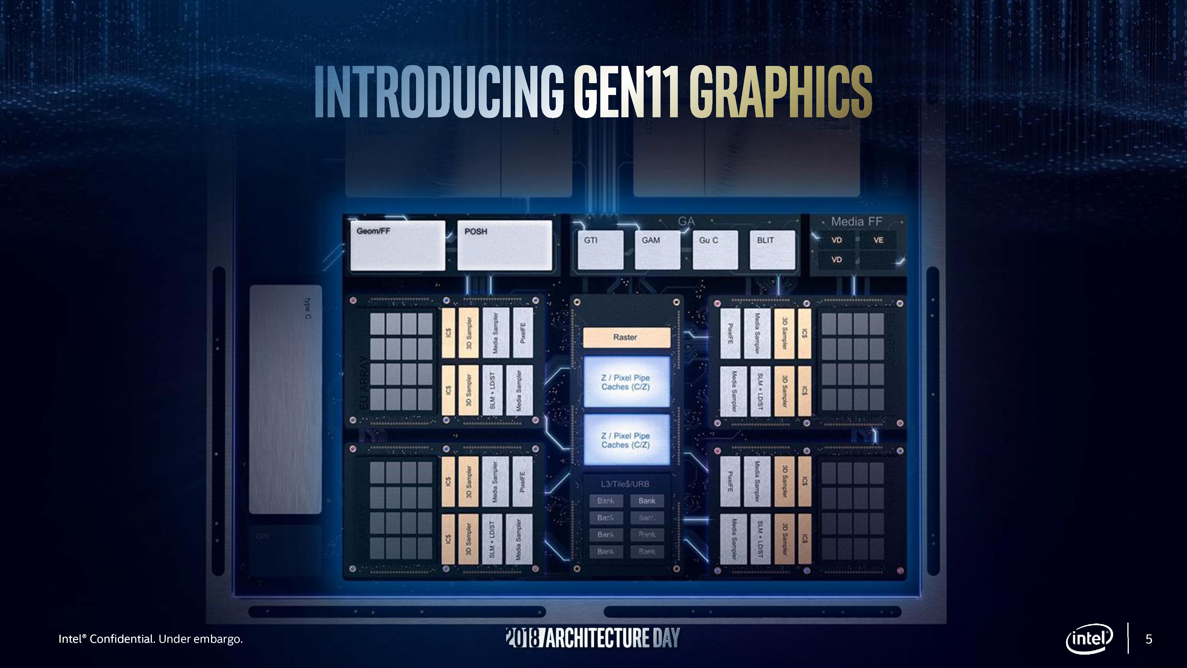
From here we can deduce a few things. We were told that this configuration is the GT2 config, which will have 64 execution units, up from 24 in Gen9.5. These 64 EUs are split into four slices, with each slice being made of two sub-slices of 8 EUs a piece. Each sub-slice will have an instruction cache and a 3D sampler, while the bigger slice gets two media samplers, a PixelFE, and additional load/store hardware. Intel lists Gen11 targeting efficiency, performance, advanced 3D and media capabilities, and a better gaming experience.
Intel didn’t go into too much detail regarding how the EUs are at higher performance, however the company did say that the FPU interfaces inside the EU are redesigned and it still has support for fast (2x) FP16 performance as seen in Gen9.5. Each EU will support seven threads as before, which means that the entire GT2 design will essentially have 512 concurrent pipelines. In order to help feed these pipes, Intel states that it has redesigned the memory interface, as well as increasing the L3 cache of the GPU to 3 MB, a 4x increase over Gen9.5, and it is now a separate block in the unslice section of the GPU.
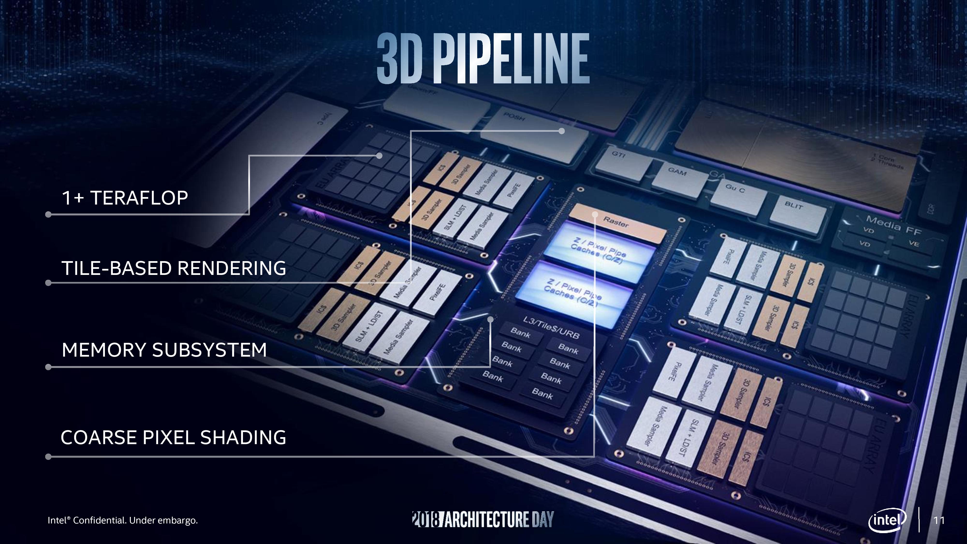
Other features include tile-based rendering, which Intel stated the graphics hardware will be able to enable/disable on a render pass basis. This will make Intel the final member of the PC GPU vendor community to implement this, following NVIDIA in 2014 and AMD in 2017. While not a panacea to all performance woes, a good tile rendering setup plays well to the bandwidth limitations of an integrated GPU. Meanwhile Intel's lossless memory compression has also improved, with Intel listing a best case performance boost of 10% or a geometric mean boost of 4%. The GTI interface now supports 64 bytes per clock read and write to increase throughput, which works with the better memory interface.
Coarse Pixel Shading, Intel's implementation of multi-rate shading and similar in scope to NVIDIA’s own Variable Pixel Shading, is also supported. This allows the GPU to reduce the amount of total shading work required by shading some pixels on a less than 1:1 basis. Intel showed two demos for CPS, where pixel shading was reduced either as a function of object distance from camera (so you do less work when things are further away), or reduced as a function of how close the object is to the center of the screen, designed to help features like foveated rendering for VR. With a 2x2 pixel stencil applied – meaning only one pixel shading operation was done per block of 4 pixels – Intel stated a ~30% increase in frame rates in supported games. Unfortunately this needs to be applied on a game-by-game basis in order to prevent significant image quality losses, so the performance gains won't be immediate or universal.
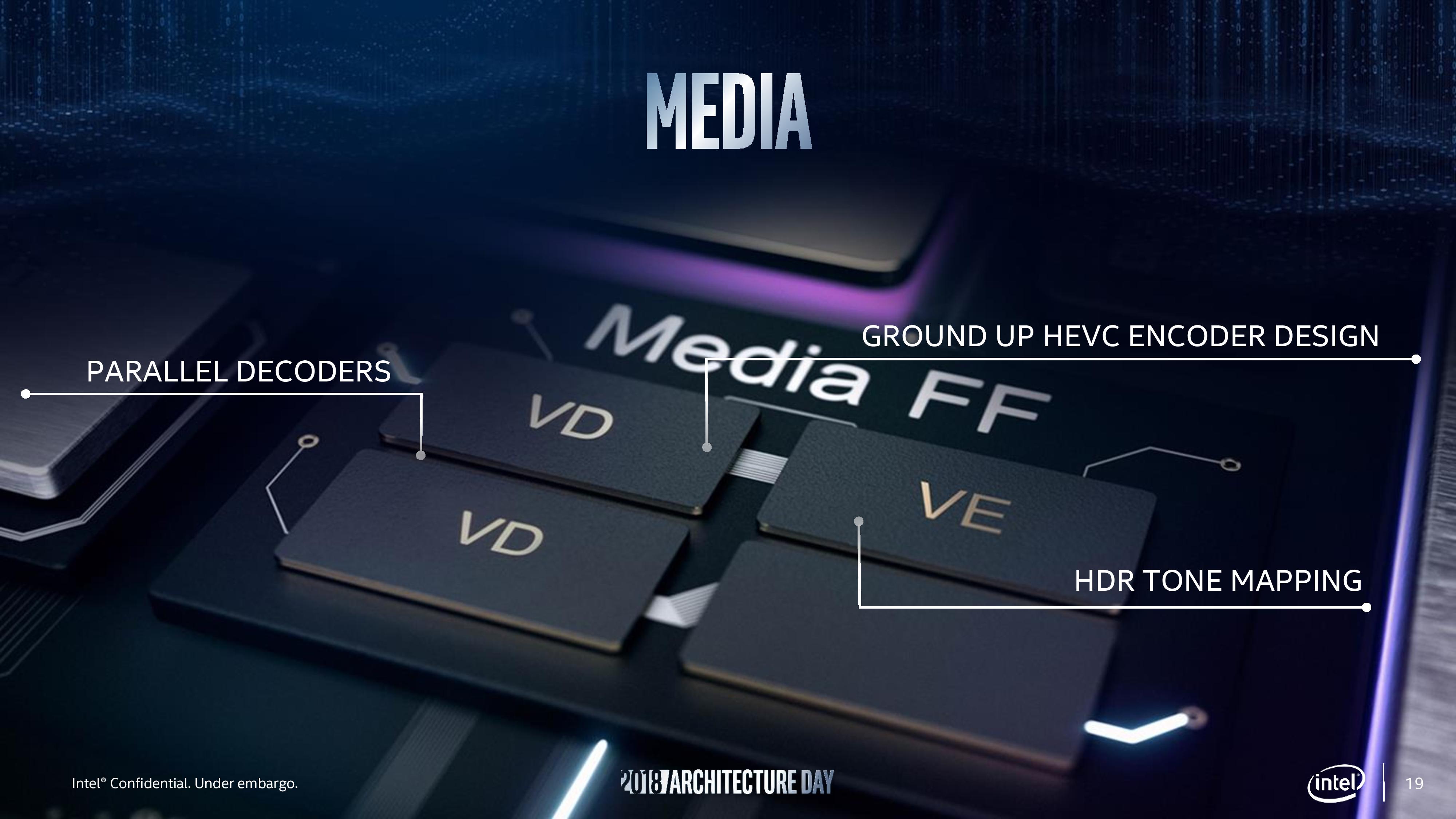
For the media block, Intel says that the Gen11 design includes a ground up HEVC encoder design, with high quality encode and decode support. Intel cited the fact that its media fixed function units are already used in the datacenter for video processing, and home users can take advantage of the same hardware. Intel also stated that by using parallel decoders it can either support concurrent video streams or they can be combined to support a single large stream, and this scalable design will allow future hardware to push the peak resolutions up to 8K and beyond.

The highlight of the display engine is support for Adaptive Sync technologies. We were told that it was announced back at the launch of Skylake, but now it is finally ready to go into Intel’s integrated graphics. This goes in hand with HDR support due to its high-precision data path.
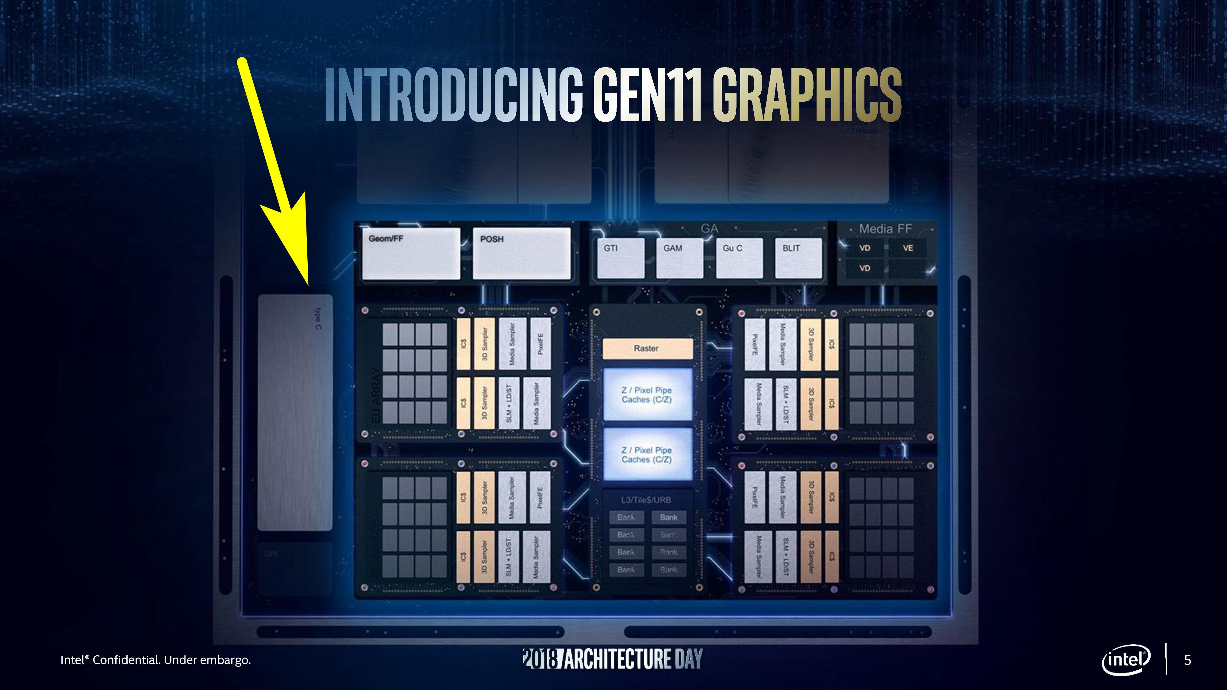
One thing in this presentation that Intel didn’t mention directly is that Gen11 graphics would appear to have Type-C video output support, potentially indicating that Intel has integrated the necessary mux into the chipset itself, removing another IC from the motherboard design.


148 Comments
View All Comments
porcupineLTD - Thursday, December 13, 2018 - link
Can you articulate what you want to say with those links? or how they might contradict me/answer my question?ajc9988 - Thursday, December 13, 2018 - link
What I am saying with those links is that AMD has already evaluated the use of active interposers and is the company that is articulating a data protocol for active interposer routing so that it doesn't matter what each chiplet does on its own data routing, so that any chiplet could be attached to an active interposer and work. Further, in the 2017 white paper, it directly shows the reason that AMD hasn't yet adopted the active interposer is due to costs. Passive interposers can be used, but don't offer the benefit of active interposers. But, the cost of an active interposer is the same as doing a monolithic chip once the active interposer is produced on the 32nm or smaller active interposer. As such, adoption did not yet make sense until the costs are reduced.https://spectrum.ieee.org/tech-talk/semiconductors...
The earlier ones show AMD did research into the optimal topology for active interposers in 2014 and 2015. It shows the optimal core count for the benefit, latencies, etc.
Now, if you look at packaging solutions, say from GF, you find that 2.5D and 3D integration is only available on 32nm and 28nm processes, with 14nm coming soon. https://www.globalfoundries.com/sites/default/file...
I bring up GF doing the packaging as, due to the WSA, even if they cost more than competitors, being able to potentially count the wafers used for the active interposers against the WSA would reduce the fines payed under that contract for doing fabrication at TSMC, making it potentially, on net, cheaper.
Now, there is an article today from Anand saying Intel is releasing the B365 chipset on 22nm. ( https://www.anandtech.com/show/13714/intel-adds-b3... ) Intel was forced to move chipsets back to 22nm due to the 10nm process not being ready for mass deployment which caused a shortage of 14nm capacity. This means Intel could not shut down their 22nm fabs to cut that capacity. As such, a fab needs to stay as close to capacity as possible or else it bleeds money (hence why AMD eventually went fabless). So, Intel using 22nm fabs to do the 22nm active interposer is just Intel making lemonade on tech that few others adopted in the industry yet due to the basis of costs. If you go back to the cost study AMD did, the active interposer at 20nm is around the cost of doing a monolithic die, which is what Intel has done to date. So it isn't really costing them more to add in the active interposer at all, while saving expenditures by keeping the 22nm fabs full of jobs, while having awesome yields on the active interposers due to it being a very mature node with low defect rates, etc. If you examine the amount of area AMD estimated is needed for the logic routers, you can see only 1%-10% area on the active interposer is needed to achieve the goal, meaning the chances a critical defect hits the active interposer is very low.
But, as to it making AMD do it, that is the wrong thinking. AMD already plans to adopt it, just not until the costs of doing so are lower. They will check the IC Knowledge lists to see when costs make sense.
But, if you look at all that data I provided, AMD has all the solutions to the problems encountered with using an active interposer. All they are waiting for is it to be cost effective. Intel isn't leading anything here, other than doing it because they need to justify and subsidize having to keep certain 22nm fabs open because of their chipsets due to the delays in 10nm. Doesn't take a genius to figure it out, just takes someone paying attention to the tea leaves.
ajc9988 - Thursday, December 13, 2018 - link
Also, I forgot to mention that the 2.5D integration of HBM Phy onto a stitched interposer was accomplished last year. This suggests that HBM could be added to an active interposer when AMD eventually does adopt an active interposer. Meanwhile, with only 1-10% of the active interposer being used according to their papers, it leaves room for in the future having elements of the I/O chip being moved to the active interposer as an additional way that things easily could develop. The question is what benefit it would be to produce what on the 32nm or 28nm nodes over having their I/O disintegrated die on 14nm. But I would bet AMD has an idea of what would be better where and will consider it when eventually adopting, considered the detailed paper on routing topology of active interposers in that group of links.porcupineLTD - Thursday, December 13, 2018 - link
Thank you for the detailed response its very informative however its besides my comment, IF Intel ships its chiplet on interposer design in 2019 they will be first (regardless of the reasons or economics behind it), as for AMD not doing it now it's again besides my comment, I wandered if they will do this for ZEN 3 or 4 not ZEN2, ZEN 3 will launch in 2020 when (as far as I know) the WSA expires so what GF does or doesn't do is not that relevant (I would be curious to know about tsmc's or samsung's packaging/interposer offerings). The result (if they implement it in ZEN3/4) will come down to cost (as you point out), socket compatibility (can it be done on the current server socket?) and planning (ZEN3 design is almost done right now so even if the interposer cost is down AMD can't implement it if they didn't predict this one year ago).porcupineLTD - Thursday, December 13, 2018 - link
Also Anandtech, I am not versed in web design, but is it really that hard to have a comment section that doesn't utterly suck? Is it really that hard to introduce an edit function, or at least a delete one?(an upvote/donvote system would be asking for too much).ajc9988 - Thursday, December 13, 2018 - link
Forgive me, many think that Intel is showing through using it that they are significantly ahead in the field of active interposers and 2.5D and 3D chiplet integration, meaning that it would take years for other chip designers to catch up, which isn't the case. So I do apologize for that assumption in regards to you.What those do show is AMD does have plans to do so in the future, it is just a matter of timing. On the socket part, there is a chance they are introducing a new socket in order to support PCIe 4.0 on the upcoming Zen 2 chips, which comes from analyzing their wording from the Next Horizon event on Nov. 6th. Meanwhile, we know that PCIe 5.0 will be finalized potentially in the first half of next year and AMD did mention DDR5 potentially being available for Epyc 3 chips based on Zen 3, but that mainstream chips will not support DDR5 in 2020 (leaves open that TR HEDT platforms may or may not get DDR5 support at that time). Intel has not provided information on when PCIe 4.0, 5.0, or DDR5 will be supported. As such, though, AMD may have backwards compatibility on the CPUs for socket compatibility, but may require a new socket for the new boards containing the new features, which I think is understandable to many in the server and workstation spheres. It is also the reason I may wait for 2020 to upgrade my 1950X rather than next year (if you are going to buy a new board, and there is a chance that board won't contain the new feature sets that release that year, waiting one more year is fine IF your workloads won't suffer for the wait).
But, I read somewhere Intel hinted at 1GB of RAM being integrated with the active interposer processors, acting as an L4 cache. Although not novel (those articles I gave for AMD whitepapers from 2014 and 2015 specifically dealt with on package integration of memory and latencies involved, suggesting we could see some type of 3d memory solution integrated when AMD does incorporate an active interposer), seeing the latencies involved with Crystalwell, which was the eDRAM on Broadwell, suggests that Intel will get a significant uplift in certain workloads, as well as keeping the chip primed and having to go off chip less often for memory calls, which is fantastic. Intel also kept the power delivery part under wraps, which is something that does excite me, but we were given no information about it (possibly bringing FIVR back, which was rumored for Ice and Tiger lake anyways).
Also, on compatibility, part of the reason I gave the article discussing data protocols for active interposers is that the routing is chiplet agnostic, meaning you can integrate parts that have their own internal routing and not effect it. Then just comes down to appropriate socket wiring, which I mentioned they may need new sockets for these features, while just maintaining drop in compatibility for consumer side.
Here is some information on other packaging types out there in the market. I am including them, but as this is just being researched, I am not attesting veracity or relevance, fully. I will have glanced through them, but you understand.
http://s3.amazonaws.com/sdieee/1817-SanDiegoCPMTDL...
"DIGITIMES reports that the new TSMC plant in Chunan will be dedicated to offering the foundry’s in-house developed advanced packaging technologies: CoWoS (chip-on-wafer-on-substrate) and integrated fan-out (InFO) wafer-level packaging, and its newly-unveiled system-on-integrated-chips (SoIC) and wafer-on-wafer (WoW) packaging services."
https://criticalmaterials.org/tsmc-to-set-up-new-f...
https://fudzilla.com/news/pc-hardware/47265-tsmc-t...
https://electroiq.com/2018/10/synopsys-design-plat...
Older article for foundational work from 2014:
https://semiengineering.com/time-to-revisit-2-5d-a...
2016 follow up: https://semiengineering.com/2-5d-becomes-real/
Packaging Market from February 2018:
http://worldherald24.com/2018/02/19/global-3d-ic-a...
Paper and slide show discussing the implementation and challenges of 3D packaging from 2016:
https://smtnet.com/library/files/upload/25d-3d-sem...
Sorry for the data dump at the end. I do apologize about that.
tommybobberson - Saturday, December 15, 2018 - link
just clarifying, do you mean to use such methods, amd would need to rive up production costs which reduces their profit/value. but since intel already has a high production cost, such methods would not affect them?ajc9988 - Wednesday, December 19, 2018 - link
tommybobberson - in a manner of speaking, yes. How much it costs to produce effects margins and pricing. One reason AMD could price the high core chips in such a manner, aside from effective yields for products, is the decreased costs to produce high core count products. If AMD added the active interposer now, it would rise production costs to be the same as a monolithic die, which would then require either an increase in market price of the products or a decrease in margins for their products.Intel, on the other hand, never captured the extra margin of going to chiplets before introducing the stacked chips. That means that the active interposer cost to them is less as the price to do so matches the cost of a monolithic die. As such, Intel can maintain their current pricing while introducing the stacked die on active interposer. Further, due to filling up 22nm fab time (because of 10nm causing a shortage of 14nm fab time which required Intel to move certain lines back to 22nm, likely forcing some plants planned to be closed or retrofitted to remain on 22nm), Intel will be able to help on the cost of 10nm delay, thereby mitigating some of the effects found in not having 10nm up and running by now.
Supercell99 - Friday, December 14, 2018 - link
With all the hackers, PC gaming is dying.sgeocla - Wednesday, December 12, 2018 - link
Fist they mock your chiplets by saying you glue your dies together, then they fail to compete with you and then years after they copy your chiplets and call it revolutionary.This is why Intel can no longer have public presentations of their own failures and have to have privately controlled presentations.