Intel's Architecture Day 2018: The Future of Core, Intel GPUs, 10nm, and Hybrid x86
by Dr. Ian Cutress on December 12, 2018 9:00 AM EST- Posted in
- CPUs
- Memory
- Intel
- GPUs
- DRAM
- Architecture
- Microarchitecture
- Xe
Sunny Cove Microarchitecture: A Peek At the Back End
One of the best parts when a new microarchitecture is announced is learning how it all works and how it has changed. Intel has been on close variants of the Skylake core since Skylake first launched in 2015, which has carried through Kaby Lake, Coffee Lake, and Coffee Lake refresh – and so getting an update to his old core design is more than welcome. While I applaud Intel for getting something new to put in front of our faces, the level of information was unfortunately less than complete. For reasons of ‘we’ll discuss more nearer the launch’, Intel was only set on discussing the back end of the microarchitecture design in any detail. In core design parlance, this means everything beyond the dispatch and order queues.
Intel framed its microarchitecture updates into two different sections: general purpose performance increases and special purpose performance increases. The company described the general purpose updates essentially as raw IPC (instructions per clock) throughput or an increase in frequency. An increase in either of these two leads to a performance increase no matter the code, at least as long as it is compute bound. Frequency is often a function of the implementation and process, whereas IPC increases can come from cores being wider (more executing instructions per clock), deeper (more parallelism per clock), and smarter (better data delivery through the front end).

The other type of performance increase is the special purpose kind, which means that certain workloads used in specific scenarios can be improved through additional acceleration methods, such as dedicated IP or specialized instructions.
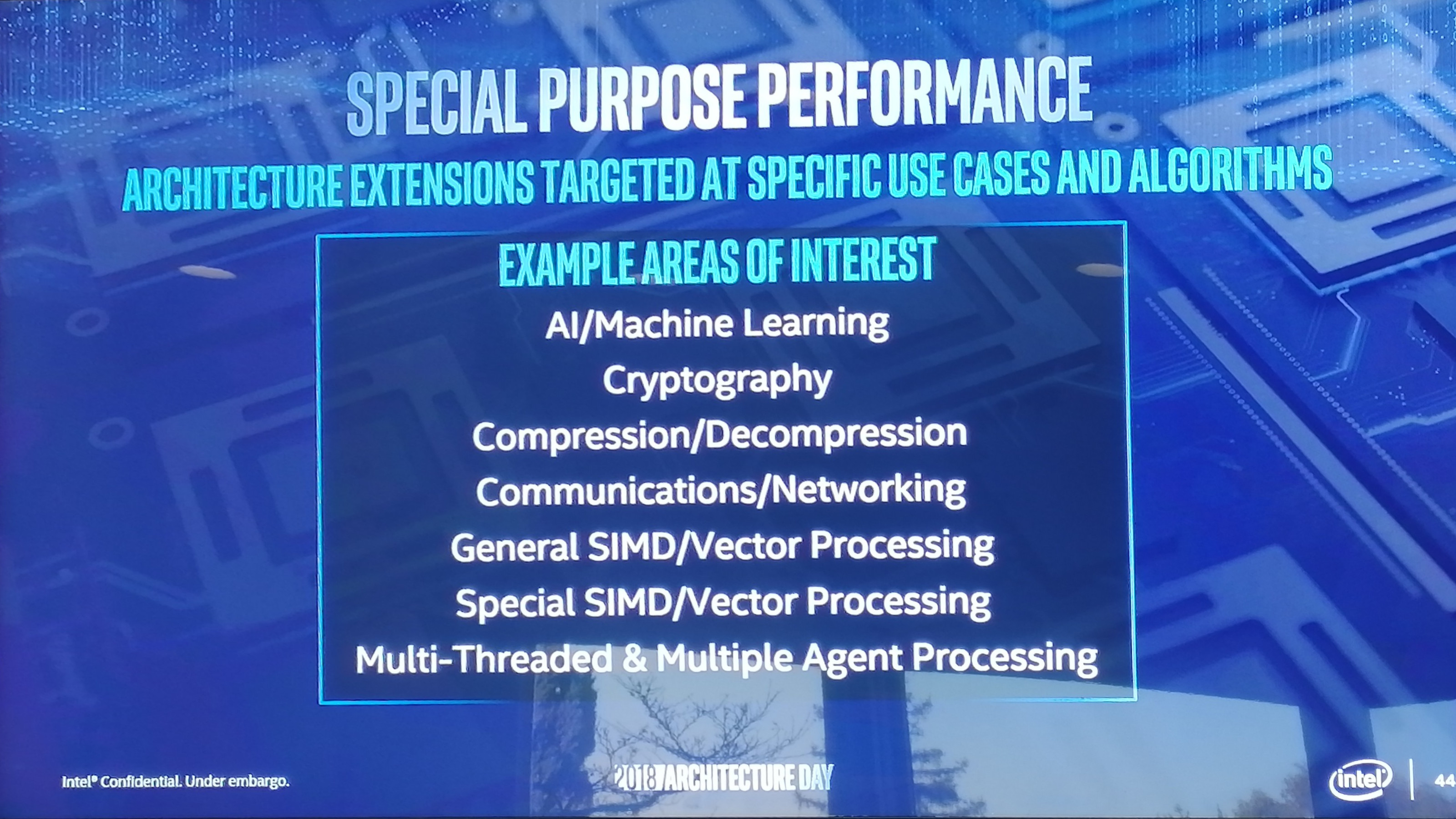
Sunny Cove is set to have both.
On the back end of the microarchitecture design, Intel has done several things including increasing cache sizes, making the execution of the core wider, increasing L1 store bandwidth, and other things.
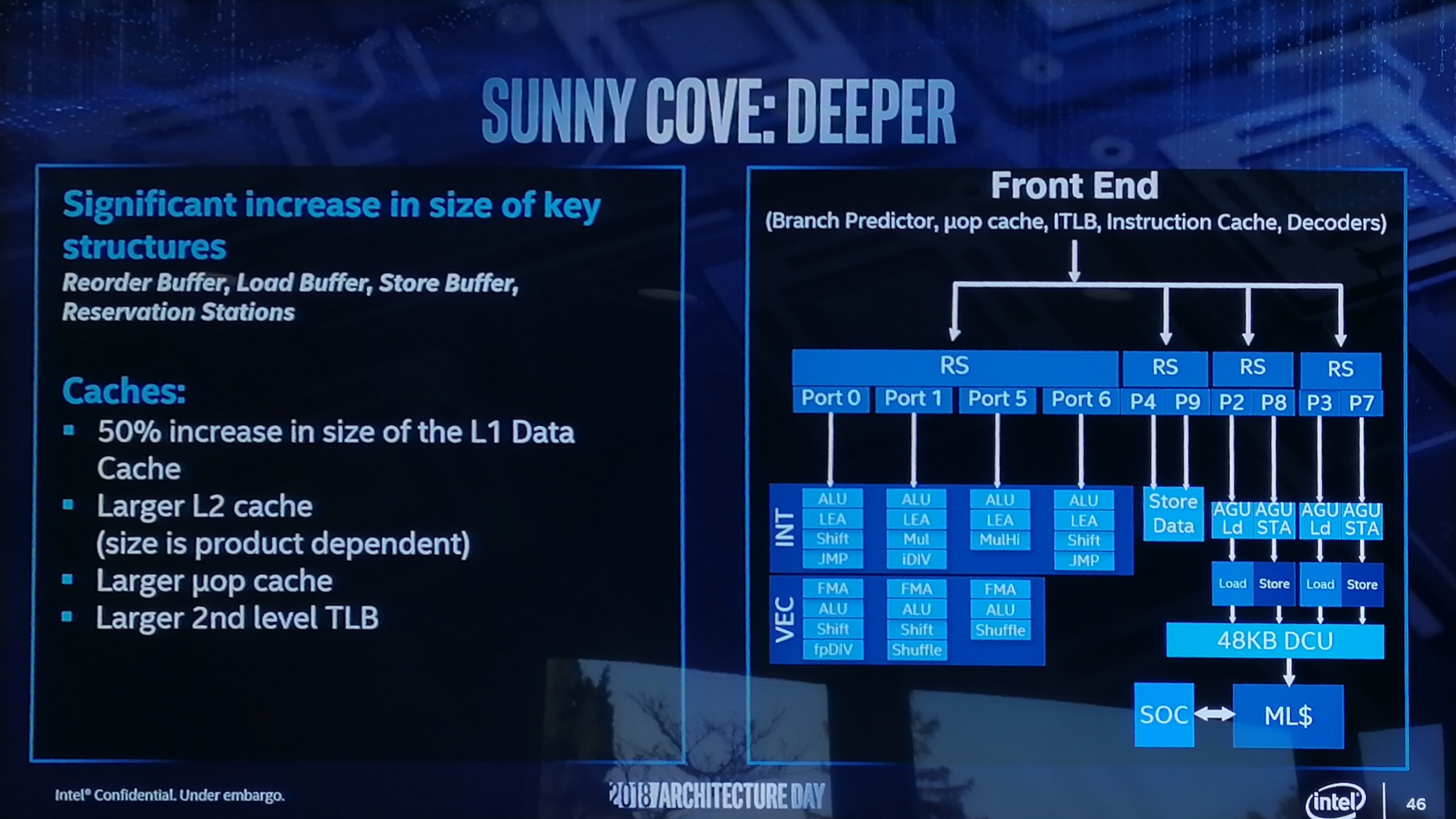
Starting with the cache improvements, the Sunny Cove core back end has a 48 KB L1 Data cache, upgraded from 32 KB. Normally cache misses decrease by a factor of a square root of the proportional size when the cache is increased, so in this case we should expect a 22% reduction in L1-Data cache misses. We are told that the L2 cache size has also been increased in both the Core and Xeon variants of Sunny Cove (256 KB and 1 MB respectively), although to exactly what size will be revealed at a later date.
While not back-end, the micro-op (uOp) cache has increased from a 2048-entry design, although exactly to what Intel is not saying at this point. The second level TLB size has also increased, which will help with machine address translation of recent addresses – normally this is increased when more lookups need to be kept and stored, which means that Intel identified a number of use cases where recent addresses had been evicted shortly before being needed.

From the diagram we can see some other changes, such as the increase in execution ports from eight to ten, allowing more instructions to come out of the schedulers at one time. Port 4 and Port 9 is linked to a cycling data store, doubling that bandwidth, but also the AGU store capabilities have doubled, for which the increased L1-D size will help. Previously on Skylake there was a potential bottleneck when all three AGUs could attempt a store, however only enough bandwidth was present for one per clock cycle. Load performance is unaffected. There is also an allocation increase, moving from four to five. This means that the dispatch out of the reorder buffer can now hit five instructions per cycle, rather than four – however given that the ops/cycle out of the Skylake decoders and uOp cache was four-to-five (depending on certain factors), it will be interesting to see how the front end has changed as a result.
There are also substantial changes in the execution ports between Skylake and Sunny Cove, which is best represented in a diagram and a table:
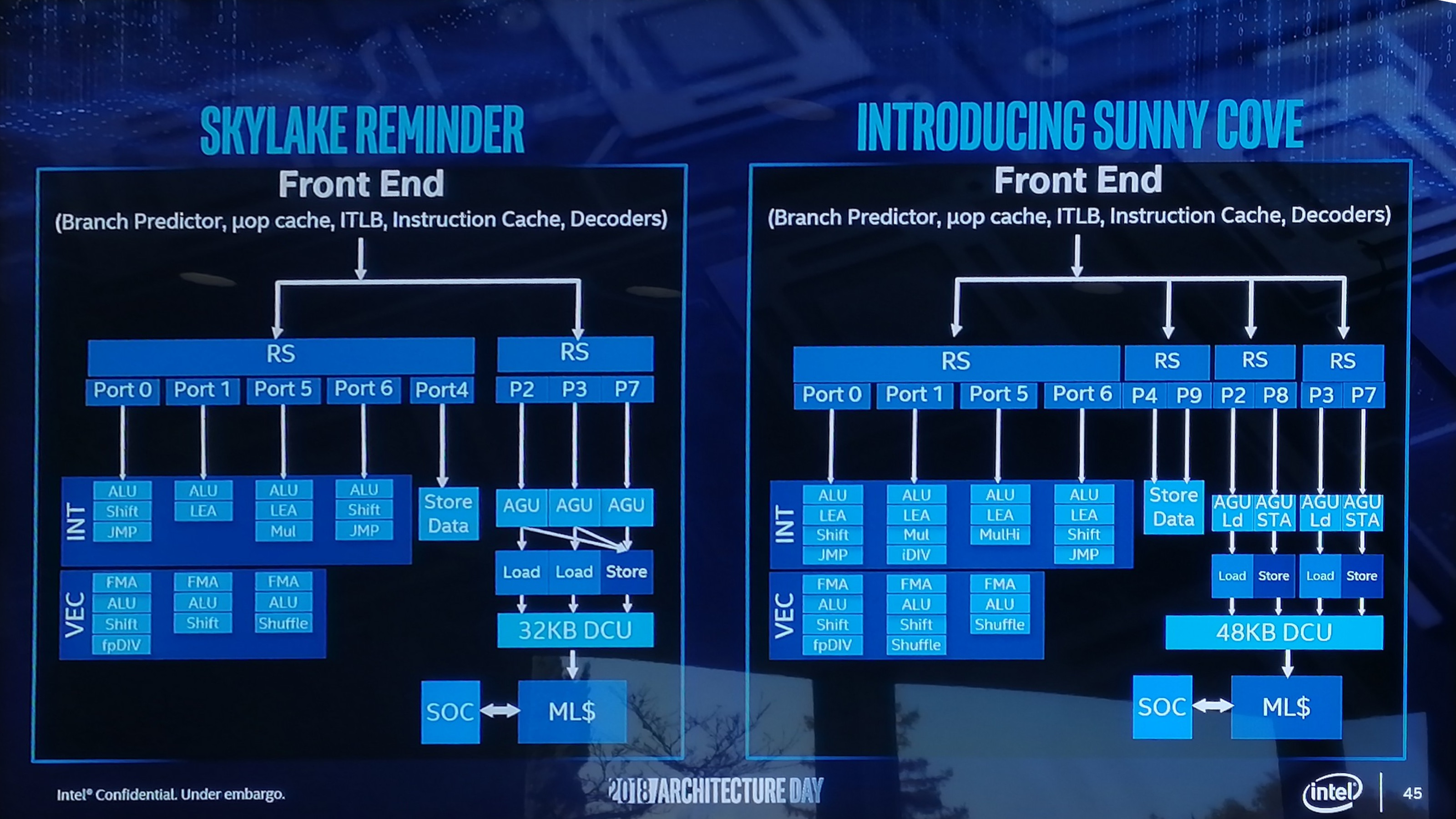
| Back-End Execution Resources | ||||||||
| Skylake | Port | Sunny Cove | ||||||
| Integer | ||||||||
| JMP | Shift | ALU | 0 | ALU | LEA | Shift | JMP | |
| LEA | ALU | 1 | ALU | LEA | Mul | iDIV | ||
| Mul | LEA | ALU | 5 | ALU | LEA | MulHi | ||
| JMP | Shift | ALU | 6 | ALU | LEA | Shift | JMP | |
| Vector / FP | ||||||||
| fpDIV | Shift | ALU | FMA | 0 | FMA | ALU | Shift | fpDIV |
| Shift | ALU | FMA | 1 | FMA | ALU | Shift | Shuffle | |
| Shuffle | ALU | FMA | 5 | FMA | ALU | Shuffle | ||
The parts highlighted in bold are different in the Sunny Cove core.
We see that Intel has equipped the Integer section of the core with more LEA units to help with memory addressing calculations, possibly to help improve performance loss with security mitigations that require frequent memory calculations or to help with high-performance array code with constant offsets. Port 1 gets the Mul unit from Skylake Port 5, probably for rebalancing purposes, but there is also an integer divider unit here. This addition is a bit of a tweak, as we know that Cannon Lake has a 64-bit IDIV unit in its design as well. In that case it brings 64-bit integer division down from 97 clocks (a mix of instructions) down to 18 clocks, and this is likely something similar. Also on the INT side is that Port 5’s multiply unit has become a ‘MulHi’ unit which in other implementations leave most-significant nibble of the result in a register for further use. I'm not sure exactly what its position is here in the Sunny Cove core though.
On the FP side, Intel has increased the shuffle resources, which we are told was because they had customers requesting this functionality to help remove bottlenecks in their code. Intel didn’t state the capabilities for the FMAs in the FP part of the core, however we do know that the core has an AVX-512 unit, so at least one of these FMAs should interface with it. Cannon Lake only has one 512-bit FMA, and that most likely carries over here, and the Xeon Scalable version might get two. I would like to get proved wrong though.
Other updates to the core as listed from Intel include improvements to the branch predictor and a reduced ‘effective load latency’ (due to the TLB and L1-D), although it was pointed out that these improvements won’t help everyone, and might require new algorithms in order to use specific parts of the core.
We’re waiting to see what changes Intel has made on the front-end, which is where a lot of low-hanging fruit often lies for performance.
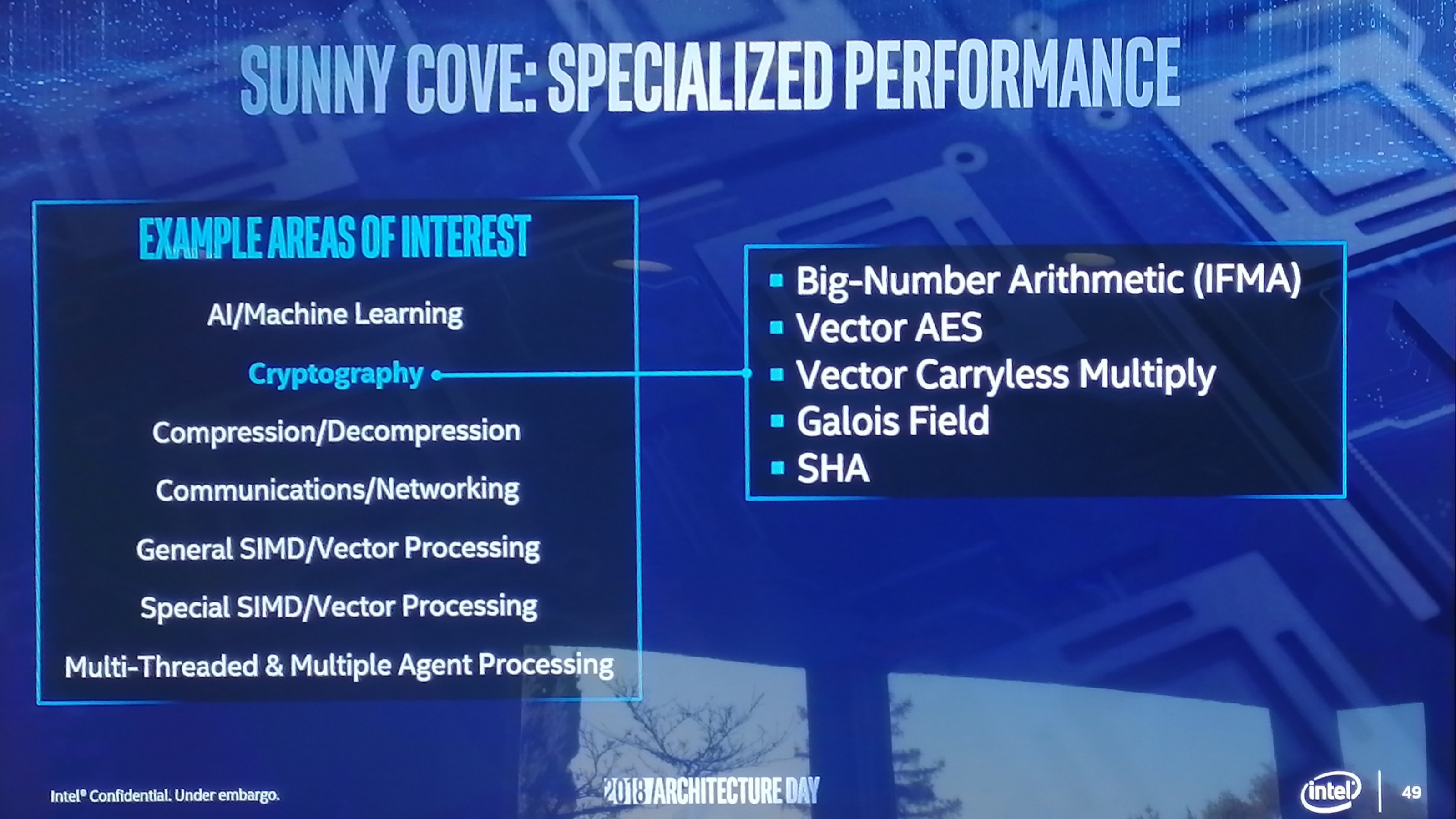
On top of the microarchitecture differences, there are new instructions for the Sunny Cove core to help speed up specialist compute tasks. With the AVX-512 unit in play, the new core will support IFMA instructions for big arithmetic compute, and which are also useful in cryptography. Along the same lines, Vector-AES (supporting more AES concurrently) and Vector Carryless Multiply are also supported. SHA and SHA-NI instructrions are also added, along with Galois Field instructions, which are fundamental building blocks in some elements of cryptography as well.
For Sunny Cove, there is also built-in support for larger memory capacities. The paging table for main memory is now a five layer design, up from four layers, supporting a Linear Address space up to 57 bits and a physical address space up to 52 bits. This means, according to Intel, that the server processors could theoretically support 4 TB of memory per socket. We will see Sunny Cove hit the market in the server space with Ice Lake-SP in 2020 according to Intel’s previous Xeon roadmaps. For security, Sunny Cove has access to Multi-Key Total Memory Encryption, and User Mode Instruction Prevention.
So where does this leave us in terms of Sunny Cove predicted performance compared to Skylake at a clock for clock level? Unfortunately we don’t have enough information. There is only enough to whet the appetite. Intel wants you (and me) to come back for more in 2019.


148 Comments
View All Comments
peevee - Tuesday, December 18, 2018 - link
"Normally cache misses decrease by a factor of a square root of the proportional size when the cache is increased"This is neither true in most performance-critical real cases nor can provide any estimate of actual performance increase.
mikato - Friday, December 21, 2018 - link
I'm here for the "raja inside" comments. Disappointed.peevee - Sunday, December 23, 2018 - link
"although it was pointed out that these improvements won’t help everyone, and might require new algorithms in order to use specific parts of the core."Which means it will help almost no one, as very few will optimize specifically for that core.
"We’re waiting to see what changes Intel has made on the front-end, which is where a lot of low-hanging fruit often lies for performance."
Low-hanging fruit in x86 was picked up in Pentium. Since then it is just more and more kludges which cost more energy than improve performance (normalizing for node).
peevee - Sunday, December 23, 2018 - link
"64 EUs... Each EU will support seven threads as before, which means that the entire GT2 design will essentially have 512 concurrent pipelines."Math?
And are these threads? Or ALUs?
peevee - Sunday, December 23, 2018 - link
"The 7-Zip demo was relatively straight forward, showing how the new instructions such as Vector-AES and SHA-NI in Sunny Cove can give the processor a 75% boost in performance over an equivalent Skylake based platform at iso-frequency."Huh? Have they recompiled (what compiler supports the new instructions then), or manually wrote a codepath in asm? And enabled encryption so to get any increase, so the increase is not actually for compression? Have they disabled compression too? ;)
dampf - Wednesday, January 2, 2019 - link
Really Intel? Adding AI improvements to Core architecture in 2021? Smartphone vendors were doing it last year... way too late. And 5G will take off in the end of 2019.TheJian - Wednesday, January 2, 2019 - link
I guess I'm not getting why I should be impressed by this.https://www.electronicsweekly.com/news/design/comm...
Leti already did it? They say it's IP can be used by others, so is this Intel's solution (what they're using I mean)?
AMD already does chiplets, everyone does socs (Intel failed them)...etc. 144mm^2 not that small (about an large apple soc size). Current 7nm A12 is 83mm^2 with 6.9B transistors and two big cores, 4 small. AMD already did interposer/chiplets. Memory has been stacking for a while now. Not sure what is supposed to impress me here.
"Very much like a mobile chip" ...Pretty much...Again, why so impressed?
And as OP noted, you have no idea how big the market is, nor how much they can make on them. I think they have to try to sell some before we can say that (many Intel things killed over the years), as their last mobile strategy cost them 16B+ in giveaways, and lost the fab race for a while (maybe forever, because that 16B lost should have went DIRECTLY into fabs and 10nm wouldn't be crap now), as once 7nm Intel hits, it looks like TSMC beats them anyway with 5nm (ok, tie? whatever). My point here is Intel's 7nm won't be much ahead of tsmc 5nm if at all as that is what it will compete with since tapeouts happen q2 2019 and chips 12-15 months later.
https://www.extremetech.com/computing/278742-tsmc-...
Many other articles out there like this, but has a good chart of when and how much wafers etc. But if risk production is really as they say, 5nm chips by xmas 2020. That puts Intel where with this @7nm? Unless that answer is XMAS 2020, I'm thinking behind tsmc. It looks like TSMC is aiming before xmas and they've been moving at a good clip without many glitches recently, so Intel better get busy IMHO. TSMC is 2q 2019 risk, or 2H 2019 depending on who you believe I guess. But still, Intel 7nm better hit by xmas 2020 then right?
Comments on last page: Uh, should have bought NV under $10 but couldn't take the best from gpu side because nobody could handle Jen as president :) WOW, look at that value you passed up Intel, oh, and you'd RULE mobile by now with all those tegras being on Intel's process 5+yrs ago (never mind what gpus would have done on Intel during this time) and you already had the modem solution too (NV bought one, and had to kill it, intel would have taken over everything cpu/gpu/modem/mobile).
With chromebooks, 2b mobile units not using NV gpu's etc, nobody would have stopped them at FTC since more gpus, and arguably more computing devices ship without WINTEL, Intel's gpus (even with NV in there) etc. Intel gpus wouldn't have been needed, mobile wouldn't have been lost (14nm Intel NV socs would have competed well against 20nm everyone else, same story before 14/20, Intel 22nm NV socs vs. 28nm everyone else)., fab money wouldn't have been blown on mobile etc etc. All the problem Intel has now are because they blew 16B on failing instead of BUYING NV for that or a bit more. They had a value back then ~6B or less 659mil shares at $10, I bought at 12...ROFL. They should have owned NV anywhere in there and all this crap wouldn't have happened...LOL. We'll see how this "ideas from outside" crap works out now. To be fair AMD had the same problems to some extent, firing Dirk for not liking mobile/tablet/apu, and wanting a KING first then that cheap crap later. Now they chase king cpu (not gpu yet so far) again...LOL. Yeah, I own AMD stock but still think management is dumb. Can't price anything right, always trying to be a friend or get share which means NOTHING if it doesn't come with MARGIN as a poor man. Sure the rich guy can flood a market, kill enemy sales, but only because he has wads of cash and can wait until he breaks you. Poor company needs NET INCOME for the next gen R&D and to retain people like KELLER etc.
I'm only in AMD stock for the 7nm server stuff, then out likely. Rumor/hype work well in advance of real product at amd (talking stock price here), so you don't likely have to wait for anything other then "shipping soon" or some leaked benchmarks etc. and the price will head to 40+ probably. Just run before that reality hits or brave the waves...LOL. I think AMD will make money, certainly has the server chips to do it, but management just seems to fail at pricing anything to take advantage while they can. Too worried about market, instead of MARGIN for R&D. I'd rather own the 10% that makes most of the money than the 80% that makes crap+a little midrange crap. Apple thinks the same, see their Q reports for ages etc. Own the rich so you can afford to supply the poor. It doesn't work the other way around generally speaking, especially as the little guy. You can't bleed as the poor little guy ;)
TheJian - Wednesday, January 2, 2019 - link
One more point, in case anyone brings it up, A12x 122mm^2 10B transistors. just adds two more big cores IIRC (maybe a few other small changes). Same point though.