The 2018 Apple iPad Pro (11-Inch) Review: Doubling Down On Performance
by Brett Howse & Andrei Frumusanu on December 4, 2018 10:00 AM ESTPowering iPad Pro: A12X
Section by Andrei Frumusanu
Apple’s new A12X SoC continues the tradition of representing an up-scaled version of the newest generation phone SoCs, in this case the A12. We’ve covered the A12 extensively in our review of the iPhone XS and XS Max, including more extensive coverage of the microarchitectural characteristics of Apple’s newest generation Vortex and Tempest cores.
The A12X, microarchitecturally, looks to be largely sharing the same generation IP blocks as the A12, with the only big difference being that the number of units has been increased in all major aspects of the SoC. Apple now for the first time employs a total of 8 CPU cores on the A12X, and compared to the A12, the figure was achieved by doubling the amount of the big Vortex cores from a dual-core to a quad-core setup. On the GPU side of things, we’ve seen the core count increase from 4 cores in the A12 to a 7-core setup in the A12X. Most important for GPU performance though – and a key aspect of the A-X series from Apple – is that the company has doubled the memory interface width 64-bit wide to 128-bit.
CPU Frequencies
In terms of CPU frequencies, Apple largely follows the same scaling pattern as on the A12, with the only difference being that there’s of course two more big cores at play. Here the A12X can support up to 8 total threads without having to resort to time-slicing their processing times.
| Maximum Frequency vs Loaded Threads Per-Core Maximum MHz |
||||||||
| Apple A12 | 1 | 2 | 3 | 4 | 5 | 6 | 7 | 8 |
| Big 1 | 2500 | 2380 | 2380 | 2380 | 2380 | 2380 | - | - |
| Big 2 | 2380 | 2380 | 2380 | 2380 | 2380 | - | - | |
| Little 1 | 1587 | 1562 | 1562 | 1538 | - | - | ||
| Little 2 | 1562 | 1562 | 1538 | - | - | |||
| Little 3 | 1562 | 1538 | - | - | ||||
| Little 4 | 1538 | - | - | |||||
| Apple A12X | 1 | 2 | 3 | 4 | 5 | 6 | 7 | 8 |
| Big 1 | 2500 | 2380 | 2325 | 2325 | 2325 | 2325 | 2325 | 2325 |
| Big 2 | 2380 | 2325 | 2325 | 2325 | 2325 | 2325 | 2325 | |
| Big 3 | 2325 | 2325 | 2325 | 2325 | 2325 | 2325 | ||
| Big 4 | 2325 | 2325 | 2325 | 2325 | 2325 | |||
| Little 1 | 1587 | 1562 | 1562 | 1538 | ||||
| Little 2 | 1562 | 1562 | 1538 | |||||
| Little 3 | 1562 | 1538 | ||||||
| Little 4 | 1538 | |||||||
On a single CPU core, the A12X clocks up to an identical 2500MHz as the A12. The similarities continue with two active big cores where the peak frequency is limited to 2380MHz. Finally, when three or four Vortex cores are active, the peak frequency on the A12X is limited to 2325MHz. The small Tempest cores see an identical frequency scaling as on the A12, with one core clocking up to 1587MHz, two to three cores at 1562MHz and finally 1538MHz when all four cores are active.
Cache Hierachy
Another way of scaling performance of a SoC is not only increasing the amount of computation blocks, but also changing aspects such as the amount of cache available to the various blocks. Let’s see if the A12X differs from the A12 in this regard:

Analysing the memory latency behaviour of the A12X and comparing it to the A12, it looks like Apple hasn’t really changed the cache configuration. The L1 caches are still at 128KB – but that was something to be expected. What is more interesting, is it seems the L2 cache also has an identical size to the A12.
The A12 L2 cache was quite unique in its behaviour in that it seemingly is of 8MB of physical size on the SoC die, however there looked to be a sort of logical partitioning in a way that a single core only has access to 6MB at fast access latencies. Furthermore in the latency graph we also see the separation of the L2 cache into two banks, with the second half of the 6MB region being slightly slower for full random access patterns.
Overall there’s a bit of a conundrum here, as we can’t really reach an accurate conclusion: Has Apple maintained the L2 cache at 8MB, or do we simply not see more of it because of a continuation of this logical partitioning? While we don’t have access to a die shot of the A12X to confirm this, I still think this is simply a case of Apple maintaining 8MB of L2 and sharing it among the four Vortex cores.
One of the A12’s big improvements was the new system level cache coming in at 8MB and employing a new microarchitecture. It looks like this part of the memory cache hierarchy has also remained unchanged as we just see minor differences in the latency behaviour past 8MB (Past the L2).
SPEC2006 Performance
We’ve extensively covered the SPEC2006 performance of the A12 in our review of the iPhone XS/XS Max and analysed the microarchitectural characteristics of the new Vortex CPU as observed in the performance results of the various SPEC workloads.
We continue the same exercise on the A12X: In general we shouldn’t expect too big variations here from the iPhone results, with the only big difference between the two SoCs being the increased memory bandwidth available to the A12X.
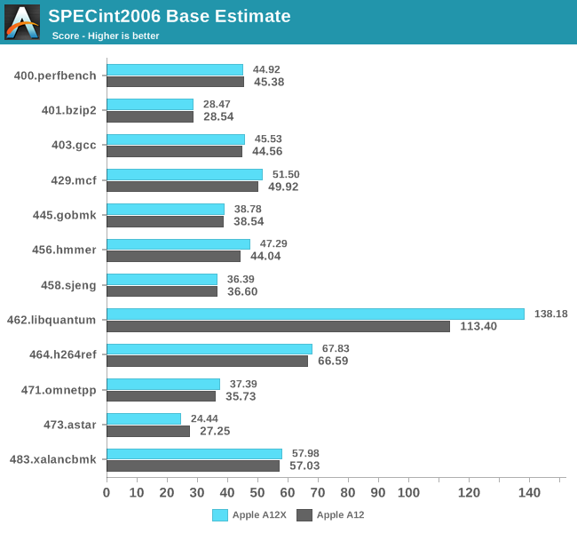
In SPECin2006, the A12X’s performance is pretty much in line with the A12, with the scores being pretty much within the margin of error, although the A12X ends up a percentage point or two faster than the A12 in some benchmarks.
The big outlier here is 462.libquantum: The benchmark workload here is characterised as heavily vectorised and extremely memory bandwidth intensive. Here the 21% increase could very well be attributed to the doubled memory bandwidth available to the A12X.
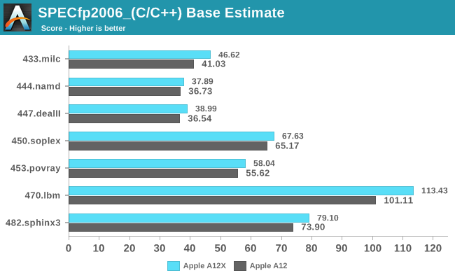
In SPECfp2006, a more significant amount of workloads are characterised by their memory and latency intensive nature. Here, the advantages of the A12X are more visible as we’re seeing an average 7% increase, ranging from 3% as the lowest increase in 444.namd up to more significant 14 and 12% increases in 433.milc and 470.lbm.
The overall SPEC2006 scores for the A12X are 45.95 in SPECint2006 and 58.78 in the C/C++ workloads of SPECfp2006 – representing 2% and 7% increases over the A12.
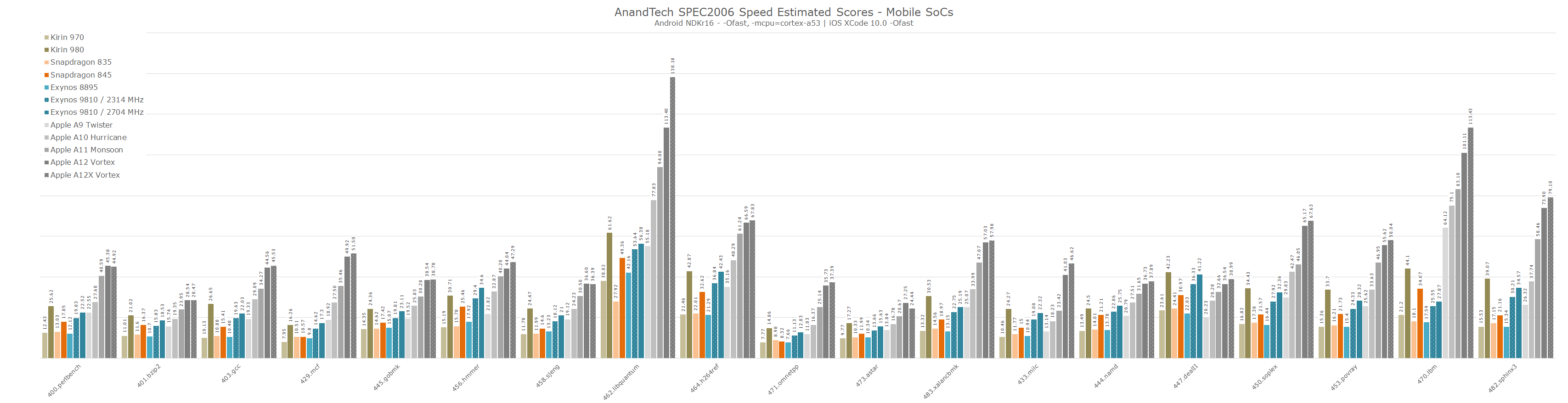
For the sake of comparison against the various existing mobile SoCs, here’s again a large graph overview comparison containing all relevant recent Arm microarchitectures.
Unfortunately for this review we weren’t able to probe the power and efficiency of the A12X – however I’m expecting figures not all too different to what we’ve published on the A12, meaning single-core active system power should be in the 3.6-4.3W range. Naturally this should be a bit higher on the A12X due to the doubled memory controller interfaces.
Overall, the A12X is a beast of a SoC and very much follows the performance of the A12. The CPU on the A12X seems pretty much the same as on the A12 – with slight performance increases in workloads that more heavily stress the memory subsystem, here the doubled memory bandwidth helps the A12X to rise above the A12.


145 Comments
View All Comments
jeremyshaw - Tuesday, December 4, 2018 - link
Crikey, that's a fast chip.That question about the xbox one s class GPU does raise questions. Why does the Xbox One S draw so much power?
axfelix - Tuesday, December 4, 2018 - link
Because it's still using an AMD GPU architecture from 2013, and Apple's and Nvidia's architectures are >3x as powerful per watt at this point.PeachNCream - Tuesday, December 4, 2018 - link
Eh, NV is just as bad. Their current gen products (GT 1030 aside) generally need more than 75W of power and occupy space equal to two PCI-E slots.Pyrate2142 - Tuesday, December 4, 2018 - link
Yeah, but those 75W and above cards are operating at a significantly higher performance. You cannot really compare it straight like rust, because 1- not only is the NV cards doing full FP32 compute compared to mixed FP16 and FP32 on the iPad, meaning it is inherently a more strenuous workload to begin with. 2- performance scaling is not a linear functionIn short we can't really take those claims at face value because A- we don't have a way to measure and compare performance in the first place (which brings me to the question of how is apple actually comparing? Using TFLOP performance? Because TFLOP is not an accurate way of measuring GPU performance as a GPU has to do more than just FLOP. Take a RX580 at almost 7 TFLOP and a similar GTX1060 6GB at 4.5TFLOP in FP32. The TFLOP difference suggests a huge performance differences butcher they both perform similarly.) and B- again NV doesn't really make cards that scale down to what the iPad is having. In short, best case it's truly an apples to oranges comparison and I don't think you can directly translate that GPU in the A12X performance against AND or NV because it just not the same comparison both in power target of even how the performance is measured
Spunjji - Wednesday, December 5, 2018 - link
Just responding firstly to endorse your comment, and secondly to note that Nvidia do make something at that scale - the 256 CUDA-core Pascal GPU in Tegra X2 would be a solid point of comparison, were it not basically impossible to perform one.olde94 - Wednesday, December 5, 2018 - link
For power/performance i have a few inputs.When looking at Nvidia jetsons running X2 and X1 most performance improvement are on the CPU side of things.
Also for power refference. The Nvidia shield is not a portable device, and the nintendo switch, running the older version of the 256 cuda core SoC have the GPU running at 764mhz in docked mode and 324 in handheld. The reason is a combination of the battery and the active 30mm fan + somewhat heatsink, cooling solution. The charger is 40W charger, and while it does charge the battery, i will assure you no more than 15W is used for this, and based on charging time during full load, it's less than 10W. Note also that the screen is NOT on.
An nvidia TX2 is rated at ~20W if i recall, making it WAY more power hungy than the A12 chip
PeachNCream - Thursday, December 6, 2018 - link
Eh, the A12X puts a lot into perspective when it comes to compute performance. The big three players in the x86 CPU and GPU space are chasing performance at a cost of rising TDP, at least the phone and tablet competition is highly constrained by power and thermal limits inherent to the platform. The result is that the technological improvements we see in those highly mobile products generally focus on both power and performance. Its a pity to see stupid dual slot coolers on graphics cards to that have to cope with TDPs that range from 75 to an absolutely irrational 200+ watts and processors that blow their TDP budget by 50% under load. I had a Packard Bell 386 PC that was happy with a 60W internal power supply. Computers in 2018 are stupid. They shouldn't even need cooling fans at this point or heatsinks. That old Packard Bell ran a bare IC without even so much as a piece of metal glued atop it and under load, you could rest your thumb on the CPU and it would feel warm, but not hot to the touch.Oliseo - Thursday, January 2, 2020 - link
That old packard bell was orders of magnitude slower than modern CPU/GPU's and was orders of magnitude less effecient than modern CPU/GPU's.Even if you normalised for cooling requirements.
This doesn't make modern CPU's/GPU's stupid, you know what it does make stupid tho....
tipoo - Tuesday, December 4, 2018 - link
It's several fabrication node shrinks back (28nm vs 7nm) and on a 2013 architecture.You could probably get something close-ish to XBO performance in a handheld Xbox on 7nm, that would be an interesting product if it had full compatibility...
axfelix - Tuesday, December 4, 2018 - link
The Xbox One S (which I think is the comparison here) is actually on 16nm, though it's still that 2013 architecture. I think Apple gets about 2/3 of the advantage from the architecture and 1/3 from the process, and it does work out still to >3x efficiency.