AMD Unveils ‘Chiplet’ Design Approach: 7nm Zen 2 Cores Meet 14 nm I/O Die
by Anton Shilov on November 6, 2018 1:53 PM EST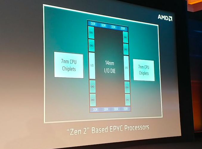
AMD on Tuesday disclosed some additional details about its upcoming codenamed Rome processor based on its Zen 2 microarchitecture. As it turns out, the company will use a new design approach with its next-generation EPYC CPUs that will involve CPU ‘chiplets’ made using TSMC’s 7 nm manufacturing technology as well as an I/O die made using a 14 nm fabrication process.
AMD’s chiplet design approach is an evolution of the company’s modular design it introduced with the original EPYC processors featuring its Zen microarchitecture. While the currently available processors use up to four Zen CPU modules, the upcoming EPYC chips will include multiple Zen 2 CPU modules (which AMD now calls ‘chiplets’) as well as an I/O die made using a mature 14 nm process technology. The I/O die will feature Infinity Fabrics to connect chiplets as well as eight DDR DRAM interfaces. Since the memory controller will now be located inside the I/O die, all CPU chiplets will have a more equal memory access latency than today’s CPU modules. Meanwhile, AMD does not list PCIe inside the I/O die, so each CPU chiplet will have its own PCIe lanes.
Separating CPU chiplets from the I/O die has its advantages because it enables AMD to make the CPU chiplets smaller as physical interfaces (such as DRAM and Infinity Fabric) do not scale that well with shrinks of process technology. Therefore, instead of making CPU chiplets bigger and more expensive to manufacture, AMD decided to incorporate DRAM and some other I/O into a separate chip. Besides lower costs, the added benefit that AMD is going to enjoy with its 7 nm chiplets is ability to easier bin new chips for needed clocks and power, which is something that is hard to estimate in case of servers.
This is a breaking news. We are updating the news story with more details.
Source: AMD


76 Comments
View All Comments
Der Keyser - Tuesday, November 6, 2018 - link
Yes Exactly - because IF needs to be much better now as there is no local low latency memorycontroller included in the CCX/Chiplet (For NUMA)ravyne - Tuesday, November 6, 2018 - link
It hasn't been said whether they'll support the AVX512 ISA, but that's not a huge deal, really. In Zen1 the FPU was 128bits wide, but there are two and they could be paired to perform 256bit AVX ops. AMD might do the same for AVX512 support in Zen2, but even if not 2x 256bit FPU is almost as good as 1x 512bit FPU in terms of throughput. The kinds of workloads that work well for wide SIMD mostly don't care how groups of lanes are partitioned, they mostly care about the total width available. Some of Intel's high-end CPUs (Xeon Gold/Platinum, the newest Xeon D, and I *think* some of the HEDT I9s have 2x 512bit FPUs, but none of them can run both at full clockspeed because power-draw is becomes too high).I wonder if 128bit SIMD performance will flatline, stagnate though. Not that anyone's serious workloads are relying on that anymore.
Rudde - Friday, November 9, 2018 - link
Another reason EPYC is cheap is manufacturing at scale. Intel manufactures a fraction XCC (extreme core count) dies compared to their mainstream processor dies. Using one small cpu die for every processor simplifies manufacturing greatly, reducing costs. A separate IO hub simplifies and reduces costs further.Alexvrb - Tuesday, November 6, 2018 - link
Hmm... I'll be interested to see what this approach could mean for future APUs. You open up a lot more possibilities with the CPU and GPU decoupled from I/O. Throw in future HBM variants and you have some interesting options, especially for mobile.CheapSushi - Tuesday, November 6, 2018 - link
I really like the look of the chiplet design package. I wonder if AMD got some help from IBM. I know they helped them with their HT implementation. Here's IBM's system controller & cores package: https://assets.pcmag.com/media/images/397587-ibm-z...catavalon21 - Tuesday, June 18, 2019 - link
First impression was how it reminded me of the L2 cache layout on my first AMD CPU, an Athlon Slot-1 K7Lolimaster - Tuesday, November 6, 2018 - link
So AMD optimized the modular arch to next level. Now improving yields even more focusing on the thing can actually be cheaper to produce the now "chiplets".AMD redifining CPU's. from going full SOC to antiSOC for high performance chips but not the obsolete monolithic design.
Lolimaster - Wednesday, November 7, 2018 - link
This could give AMD an edge on ultraportables, or the return to 10" tablets with full windows inside.Small single 4core-CCX+GPU chiclet + basic IO since the form factor of mobile devices don't need as much complexity.
Lolimaster - Wednesday, November 7, 2018 - link
This redisign goes beyond anyones imagination for Zen2 and beyond. No one expected that they weill tweak to such extreme a way of making cpu's that was supposed to be impressive yield wise. Not that 1st option went to the toilet of obsolescence.Flying Aardvark - Wednesday, November 7, 2018 - link
AMD nailed this. Far more impressive than I thought Zen2 would be. Though Zen over delivered as well, and that's why I've had a 1700, 1800X and 2700X. For consumer chips, the future is going to continue to move towards mobile, where further GPU integration and big core / little core arrangements are going to continue to be the future.