AMD Unveils ‘Chiplet’ Design Approach: 7nm Zen 2 Cores Meet 14 nm I/O Die
by Anton Shilov on November 6, 2018 1:53 PM EST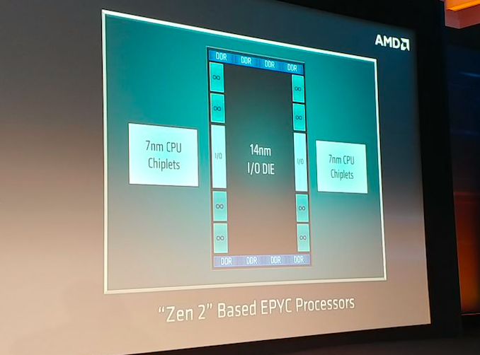
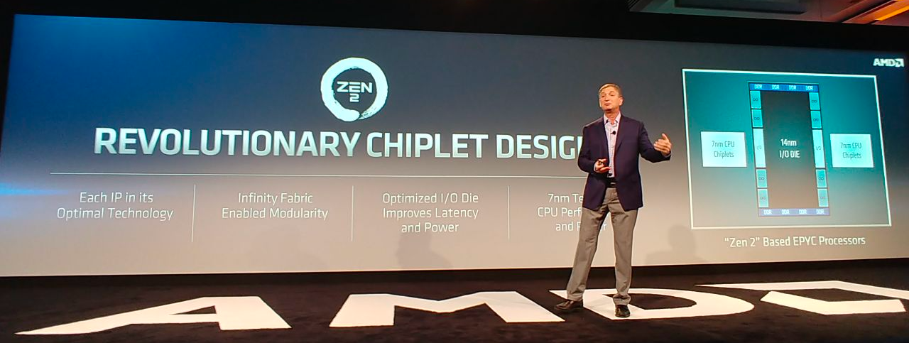
AMD on Tuesday disclosed some additional details about its upcoming codenamed Rome processor based on its Zen 2 microarchitecture. As it turns out, the company will use a new design approach with its next-generation EPYC CPUs that will involve CPU ‘chiplets’ made using TSMC’s 7 nm manufacturing technology as well as an I/O die made using a 14 nm fabrication process.
AMD’s chiplet design approach is an evolution of the company’s modular design it introduced with the original EPYC processors featuring its Zen microarchitecture. While the currently available processors use up to four Zen CPU modules, the upcoming EPYC chips will include multiple Zen 2 CPU modules (which AMD now calls ‘chiplets’) as well as an I/O die made using a mature 14 nm process technology. The I/O die will feature Infinity Fabrics to connect chiplets as well as eight DDR DRAM interfaces. Since the memory controller will now be located inside the I/O die, all CPU chiplets will have a more equal memory access latency than today’s CPU modules. Meanwhile, AMD does not list PCIe inside the I/O die, so each CPU chiplet will have its own PCIe lanes.
Separating CPU chiplets from the I/O die has its advantages because it enables AMD to make the CPU chiplets smaller as physical interfaces (such as DRAM and Infinity Fabric) do not scale that well with shrinks of process technology. Therefore, instead of making CPU chiplets bigger and more expensive to manufacture, AMD decided to incorporate DRAM and some other I/O into a separate chip. Besides lower costs, the added benefit that AMD is going to enjoy with its 7 nm chiplets is ability to easier bin new chips for needed clocks and power, which is something that is hard to estimate in case of servers.
This is a breaking news. We are updating the news story with more details.
Source: AMD


76 Comments
View All Comments
Thorgil - Thursday, November 8, 2018 - link
Plus, let's not forget that AMD have an agreement with GloFo. For every wafer they get from TSMC, they pay a comission to GloFo. With the I/O die on GloFo 14 nm process, it's also a financial factor that comes into play; why pay even more (more than just the cost of the wafer/process) for TSMC's 7nm, when GloFo 14 nm will do just as well. It's a very logical decision from a company standpoint.SleepyFE - Thursday, November 8, 2018 - link
I think they are no longer as tight. GloFo gave up on chasing super new tech and is focusing on being a more general chip maker, leaving AMD to use TSMC more anyway.Now that i read my statement i realize you are right. What is left of the contract that requires AMD to use GloFo will be used up with 14nm with a likely discount.
levizx - Saturday, November 10, 2018 - link
They only pay for "certain" wafers, not all. We don't know the details, but AMD would be extremely stupid if they agree to pay GloFo while outsourcing wafers GloFo can't even produce, especially now that GloFo don't even have a 7nm process anymore.I'd say AMD would only have to pay GloFo if they use 16/14/12/11/10 nm wafers outside GloFo.
lefty2 - Wednesday, November 7, 2018 - link
I wonder if that's true, because there was no problem scaling from 28nm to 14nm.Alistair - Tuesday, November 6, 2018 - link
so the answer to your comment is no, it doesn't make much differenceaxfelix - Tuesday, November 6, 2018 - link
A lot of the reporting on AMD's recent comeback has effectively omitted the fact that they're still really bad at low TDPs (and frankly even Intel has been getting crushed here by ARM chips, specifically Apple's, for the past couple years), so as long as they aren't trying to compete outside of desktops and servers, this isn't a huge concern.PeachNCream - Tuesday, November 6, 2018 - link
Yup, that's what bothers me about the change. Anandtech has done power measurements and the IF in TR2 processors seems to account for a good 50+W TDP of the total chip package. Not moving IF to 7nm means the 50+W TDP will remain constant (adding DRAM controllers to the mix as well so the IF "die" will eat up more TDP) while the new chiplets containing the CPUs draw less power for a given amount of work thanks to the node shrink.namechamps - Tuesday, November 6, 2018 - link
AMD can always shrink the IO hub to 7nm later. Either as a mid cycle refresh or as part of Zen 3. Right now yields on 7nm are going to be riskier and defects in the IO hub portion would axe the processor so put that on the "safe" high yield 14nm process. It now makes the cores tiny (well under 100 mm2) so even with higher defect rates on 7nm AMD should be able to crank them out by the truckload.Lolimaster - Wednesday, November 7, 2018 - link
It's gonna be funny to see prices of Ryzen 3000 next year, they could easily go now for $200-250 8 cores.Lolimaster - Wednesday, November 7, 2018 - link
Reminds me of the Xbox 360 SOC after the 1st update, update in parts.