The Mate 20 & Mate 20 Pro Review: Kirin 980 Powering Two Contrasting Devices
by Andrei Frumusanu on November 16, 2018 8:10 AM EST- Posted in
- Smartphones
- Huawei
- Mobile
- Kirin 980
- Mate 20
- Mate 20 Pro
The Kirin 980 - A Recap Overview
The Kirin 980 is the follow-up to last year’s Kirin 970. In many ways, the Kirin 980 is a much more significant chip than the previous generation chipsets from Huawei. The one thing that didn’t make the Kirin 960 and 970 as attractive, was their release schedule. The Kirin 960 suffered from being released on a 16FFC manufacturing node in a year where Qualcomm and Samsung released 10LPE SoCs – and this disadvantage for the Kirin 960 was most notable in the power and efficiency of the chipset, and was directly translated into devices which lagged behind the competition.
The Kirin 970, while closing the gap in terms of manufacturing node, on the other hand wasn’t able to catch Arm’s newest generation CPU designs due to its earlier design cycle. This meant that the chip still had to make due with Cortex A73’s versus Qualcomm’s competing Snapdragon 845 which was able to take advantage of the new Cortex A75 and A55 improvements.
This generation, HiSilicon was able to finally get manufacturing and IP design back in sync, and the Kirin 980 looks to repeat the success of the Kirin 950 from a few years ago.
| HiSilicon High-End Kirin SoC Lineup | |||
| SoC | Kirin 980 | Kirin 970 | Kirin 960 |
| CPU | 2x A76 @ 2.60 GHz 2x A76 @ 1.92 GHz @ 512KB L2's 4x A55 @ 1.80 GHz @ 128KB L2's 4MB DSU L3 |
4x A73 @ 2.36 GHz 4x A53 @ 1.84 GHz 2MB L2 |
4x A73 @ 2.36GHz 4x A53 @ 1.84GHz 2MB L2 |
| GPU | ARM Mali-G76MP10 @ 720 MHz |
ARM Mali-G72MP12 @ 746 MHz |
ARM Mali-G71MP8 @ 1037MHz |
| LPDDR4 Memory |
4x 16-bit CH LPDDR4X @ 2133MHz 34.1GB/s |
4x 16-bit CH LPDDR4X @ 1833 MHz 29.9GB/s |
4x 16-bit CH LPDDR4 @ 1866MHz 29.9GB/s |
| Storage I/F | UFS 2.1 | UFS 2.1 | UFS 2.1 |
| ISP/Camera | New Dual ISP +46% speed 10-bit pipeline |
Dual 14-bit ISP | Dual 14-bit ISP (Improved) |
| Encode/Decode | 2160p60 Decode 2160p30 Encode :( |
2160p60 Decode 2160p30 Encode |
1080p H.264 Decode & Encode 2160p30 HEVC Decode |
| Integrated Modem | Kirin 980 Integrated LTE (Category 21/18) DL = 1400 Mbps 4x4 MIMO 3x20MHz CA, 256-QAM (5CA no MIMO) UL = 200 Mbps 2x2 MIMO 1x20MHz CA, 256-QAM |
Kirin 970 Integrated LTE (Category 18/13) DL = 1200 Mbps 5x20MHz CA, 256-QAM UL = 150 Mbps 2x20MHz CA, 64-QAM |
Kirin 960 Integrated LTE (Category 12/13) DL = 600Mbps 4x20MHz CA, 64-QAM UL = 150Mbps 2x20MHz CA, 64-QAM |
| Sensor Hub | i8 | i7 | i6 |
| NPU | Dual @ >2x perf | Yes | No |
| Mfc. Process | TSMC 7nm | TSMC 10nm | TSMC 16nm FFC |
The new chipset sports Arm’s newest generation Cortex A76 CPUs: We covered the A76 earlier in the year, and the new Arm CPU represents a from the ground-up newly designed microarchitecture that promises great leaps in terms of performance, all while maintaining power efficiency.
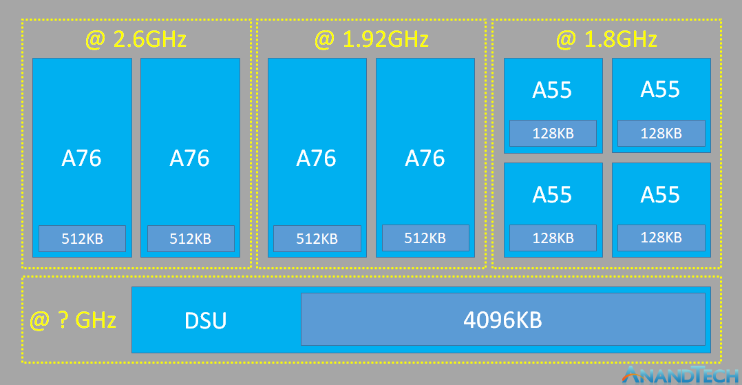
The CPU complex is based on Arm’s DynamIQ cluster architecture, and we find eight cores all in all. In terms of performance cores, we find two pairs of Cortex A76’s: One pair clocks at up to 2.6GHz, while the other pair clocks at up to 1.92GHz. HiSilicon clocks the two pairs differently for two reasons: First of all, the new A76 core does go to higher power levels than previous generation cores. This means that in a mobile smartphone design, running the four cores at maximum frequency is no longer something that is feasible as it would go beyond the sustainable TDP of the platform. In order to counter-act this, the four cores are split into two clock and voltage planes, fully taking advantage of Arm’s DynamIQ cluster allowing for this. Thus, this configuration still allows for some of the cores to achieve the maximum single-threaded performance, all while reducing the power from the other pair, to remain within reasonable TDPs.
Another advantage of this configuration is that in mixed workload scenarios, the two pairs can operate at different efficiency points independently from each other, and this would allow for energy savings in workloads where there’s either one or two high-load threads, alongside some more medium load threads that would then all onto the lesser clocked A76 pair.
Alongside the four A76’s, we find four Cortex A55 cores that are dedicated for high efficiency and lower-load workloads.
In terms of cache hierarchy, HiSilicon opted for the maximum configuration for the Cortex A76’s, configuring both pairs with 512KB of L2 cache for each core. The A55 cores sported a more mid-sized 128KB L2 caches for each core. Finally, the DSU is configured with a 4MB L3, which is double the size of the previous L2 of the Kirin 970, and also double the size of the L3 of the Snapdragon 845.
A very small flagship SoC
ChipRebel is a new player in the die shot imaging business trying to get more exposure. Most notably I was impressed by the quality of their free A11 die shot last year. I’ve been talking to the folks over there and asked them what they had in plan – and fortunately enough they were able to look into publishing a teaser die shot of the Kirin 980 on their blog, alongside a teardown of the Mate 20 as well as their commercial high-resolution poly image.
I’ve already posted a quick analysis in a dedicated pipeline post last week, but let’s go over the details of the die shot again:
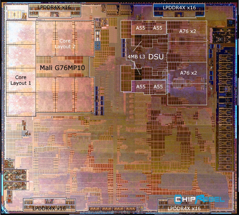
Die shot credit: ChipRebel
Again, the biggest surprise here comes in terms of the overall die size of the Kirin 980, coming in at a meagre 74.13mm², which represents a 30% reduction of last year’s Kirin 970, which came in at 96.72mm². HiSilicon uses the highest flagship Kirin SoCs in a much wider range of smartphone tiers than what we’re used to, say, Qualcomm’s or Samsung’s SoCs. As such we see a lot of Honor mid-range to “premium” devices sporting the chipsets. Thus it’s quite natural that HiSilicon wants to keep the die size to a minimum, and to extract the best value possible out of the new generation process node. Still, the small die size does come as quite a surprise, and it looks like there’s room to grow in terms of a follow-up to the Kirin 980 on the same process node.
On the top left corner we can see the new Mali G76MP10 GPU. The Mali G76 drastically differs from past generation Arm GPUs in that it essentially doubles the computational capabilities of each core – in effect that one could say that the new MP10 core configuration in the Kirin 980 is about equivalent to a MP20 of the previous generation – microarchitectural improvements aside. Here HiSilicon has kept the GPU to a size of 11.97mm², among the smallest configurations we’ve seen from the vendor, and about in line with what usually Qualcomm dedicates to its Adreno GPUs in terms of block size.
On the top right, we see the CPU complex we’ve previously discussed. Here we identify the four Cortex A76 cores, with distinctive grouping into two different pairs. The distinction between the two pairs here is due to them having different physical implementations: The high frequency pair is likely synthesized to be able to achieve a higher frequency with a greater cost in power, while the lower frequency pair is optimised for power consumption, only able to achieve a lower maximum frequency.
In terms of size, the Cortex A76 cores are still largely very tiny. With the 512KB per-core L2 cache included, an A76 core measures a meagre 1.26mm², a lot smaller than the Apple A12’s Vortex core (without L2) which comes in at 2.07mm², and also a fraction of the size of Samsung’s 10nm Exynos M3 Meerkat core with the same size L2, which came in at 3.5mm² (2.52mm² without the L2).
Improved memory latencies
The memory subsystem of a SoC is fundamental to the performance of its IP blocks. The Kirin 970 here suffered a bit as it seemingly had some issues when operating at higher clock speeds, and why Huawei had opted by default to reduce the frequency in its devices. This resulted in some performance degradations, especially in memory latency sensitive workloads, as the other consequence would have been increased power consumption.
While we already know the cache sizes of the Kirin 980, as they were officially disclosed by HiSilicon, it’s still interesting to see the cache latency differences and what kind of improvements we expect to see.
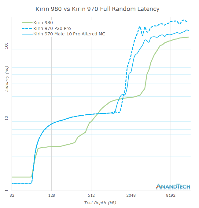
Versus the Kirin 970, one thing that’s immediately to note is that DRAM latency has been significantly improved, especially over the stock behaviour of the Kirin 970. The test we’re using here is full random latency which includes all possible penalties such as TLB misses – however this is still an important metric for performance.
The private L2 cache latency of the new Cortex A76 cores are outstanding, coming in at just 4ns, less than half of the shared L2 cache latencies of the Cortex A73 in the Kirin 970. The L3 does run asynchronously to the cores and thus it sees a latency penalty, but this is still within reasonable limits.
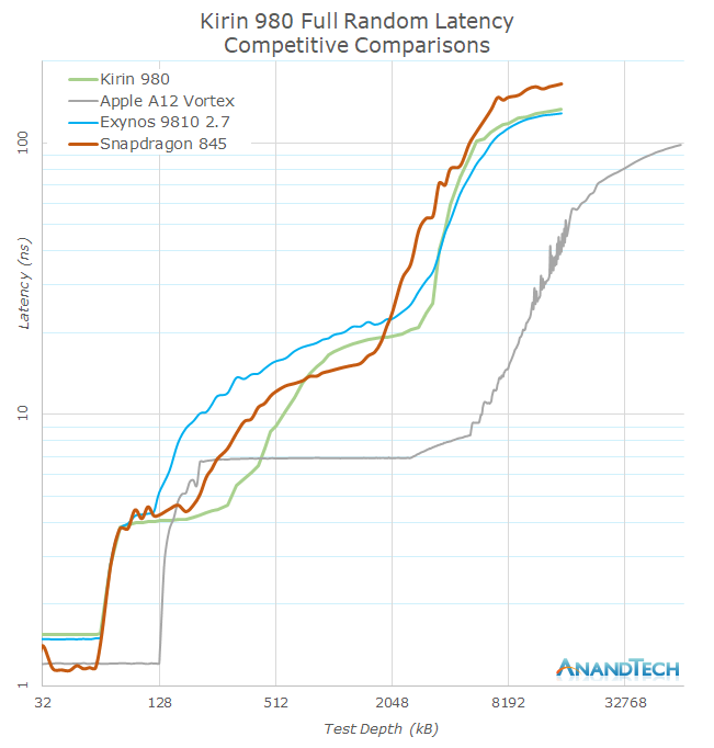
Compared the Kirin 980 against other SoCs, we see the new design compete very well against its Android counter-parts. Interesting to see is that the L3 of the Kirin 980 seems slower than that of the Snapdragon 845, so it’s possible that HiSilicon is clocking the L3 slightly slower. The Exynos 9810 has a slight advantage in DRAM memory latency, but this quickly disappears when the core is running at more reasonable frequencies. Here we also see the Exynos suffer the worst latencies throughout its cache hierarchy.
Unfortunately for the Android SoCs, Apple’s A12 is far ahead when it comes to both cache latencies as well DRAM latency, showcasing massive advantages throughout all metrics and depths, putting the other SoCs to shame.


141 Comments
View All Comments
AkiraAkimoto - Saturday, November 17, 2018 - link
Andrei will it be ok for me to translate this article into Chinese and post it on some of the Chinese forums with your name and original web link (this page) on it?s.yu - Tuesday, November 20, 2018 - link
lol, many media outlets in China already use Anandtech's content, those who mention the source are already the decent ones.AkiraAkimoto - Tuesday, November 20, 2018 - link
shameless and use partial of the content to support their "paid of view"thats how most chinese media work lol
Lukas Dvorok - Saturday, November 17, 2018 - link
Excellent and really retailed review. Thank you. Pitty that you haven't been able to test also unit with BOE display and Mate 20X.dudedud - Saturday, November 17, 2018 - link
So right now there's no reliable way to compare this kirin NPU against Apple's?And i hope that you could add the A55' SPEC scores too in the near future
ianbergman - Saturday, November 17, 2018 - link
I've only had my Mate 20 Pro for a couple of days, but interestingly, I don't see any of the display issues mentioned. And really crossing my fingers I don't! I still remember the horror of the Pixel 2 XL's hue shift. So far everything else is great - need to live with it a while to get a sense of battery in real world situations, speakers and voice quality, etc.ianbergman - Sunday, November 18, 2018 - link
If anyone knows of a great well to tell if I have an LG panel or not - would appreciate it! CPU-Z and other similar hardware info tools can't seem to tellLukas Dvorok - Monday, November 19, 2018 - link
Device Info HW application. Right on first page when you open app. Something called like touch device or so. I got LG, now I got replacement with BOE.zeeBomb - Sunday, November 18, 2018 - link
Andrei dropping us with that GREAT REVIEWS!!!Lukas Dvorok - Sunday, November 18, 2018 - link
Hello, will reducing resolution on Mate 20 PRO to FHD+ mitigate higher power drain caused by dual MIPI lane? Thank you